Datasheet Details
| Part number | SN74LV11A |
|---|---|
| Manufacturer | Texas Instruments |
| File Size | 967.56 KB |
| Description | TRIPLE 3-INPUT POSITIVE-AND GATES |
| Datasheet |
 SN74LV11A-etcTI.pdf SN74LV11A-etcTI.pdf
|
| Part number | SN74LV11A |
|---|---|
| Manufacturer | Texas Instruments |
| File Size | 967.56 KB |
| Description | TRIPLE 3-INPUT POSITIVE-AND GATES |
| Datasheet |
SN74LV11A-etcTI.pdf
|
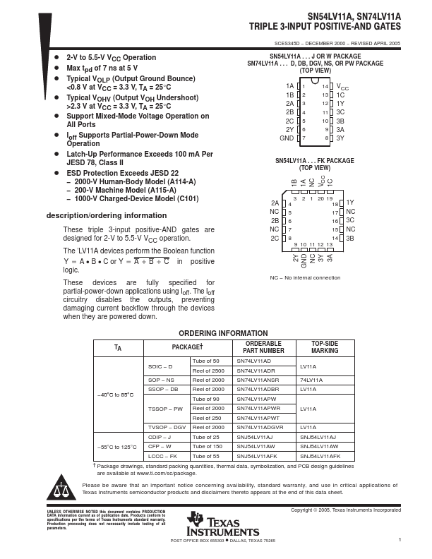
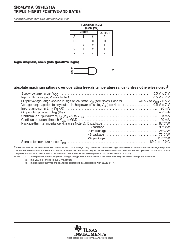
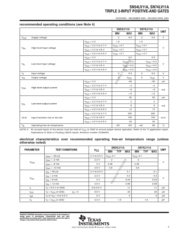
ordering information These triple 3-input positive-AND gates are designed for 2-V to 5.5-V VCC operation.The ’LV11A devices perform the Boolean function Y + A B C or Y + A ) B ) C in positive logic. DECEMBER 2000 REVISED APRIL 2005 SN54LV11A
📁 SN74LV11A Similar Datasheet