Datasheet4U Logo Datasheet4U.com

SN74LVC112A Dual Negative-Edge-Triggered J-K Flip-Flop

📥 Download Datasheet  Datasheet Preview Page 1

Description

Product Folder Sample & Buy Technical Documents Tools & Software Support & Community SN74LVC112A SCAS289M * JANUARY 1993 * REVISE.
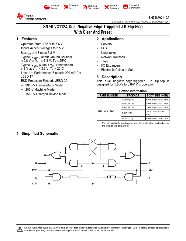
This dual negative-edge-triggered J-K flip-flop is designed for 1.

📥 Download Datasheet

Preview of SN74LVC112A PDF
datasheet Preview Page 2 datasheet Preview Page 3

Features

* 1 Operates From 1.65 V to 3.6 V
* Inputs Accept Voltages to 5.5 V
* Max tpd of 4.8 ns at 3.3 V
* Typical VOLP (Output Ground Bounce) < 0.8 V at VCC = 3.3 V, TA = 25°C
* Typical VOHV (Output VOH Undershoot) > 2 V at VCC = 3.3 V, TA = 25°C
* Latch-Up Pe

Applications

* Servers
* PCs
* Notebooks
* Network switches
* Toys
* I/O Expanders

SN74LVC112A Distributors

📁 Related Datasheet

  • SN74LVC1G125 - high performance non-inverting buffer (UMW)
  • SN74LVC1G34 - Single buffer (UMW)
  • SN74L71 - AND-Gate R-S Master-Slave F-F (National Semiconductor)
  • SN74L74N - Dual D-Type Flip-Flop (ETC)
  • SN74LS00 - QUAD 2-INPUT NAND GATE (Motorola)
  • SN74LS02 - QUAD 2-INPUT NOR GATE (Motorola)

📌 All Tags

Texas Instruments SN74LVC112A-like datasheet