Click to expand full text
www.ti.com
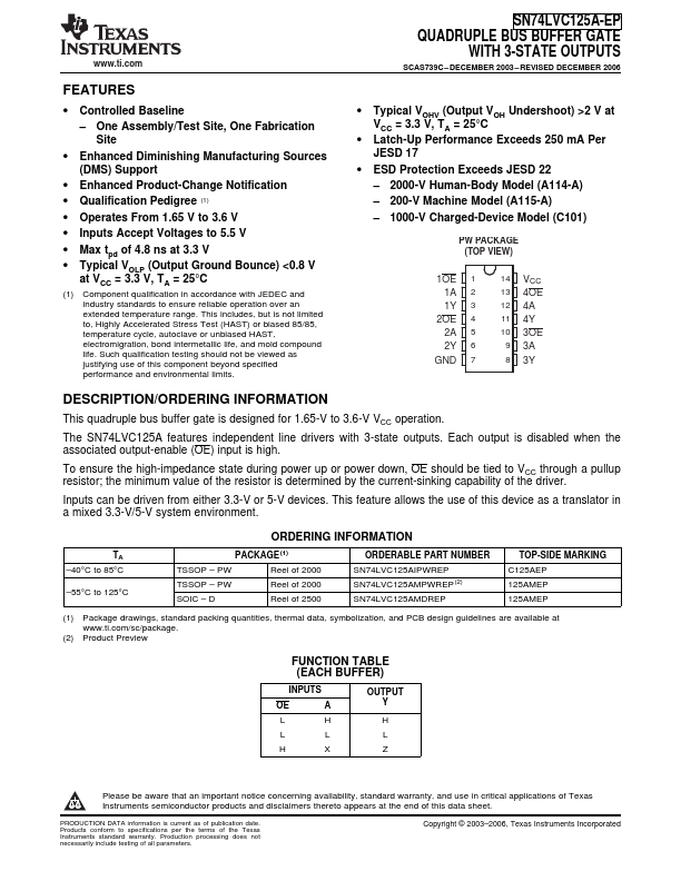
FEATURES
• Controlled Baseline
– One Assembly/Test Site, One Fabrication Site
• Enhanced Diminishing Manufacturing Sources (DMS) Support
• Enhanced Product-Change Notification • Qualification Pedigree (1) • Operates From 1.65 V to 3.6 V • Inputs Accept Voltages to 5.5 V • Max tpd of 4.8 ns at 3.3 V • Typical VOLP (Output Ground Bounce) <0.8 V
at VCC = 3.3 V, TA = 25°C
(1) Component qualification in accordance with JEDEC and industry standards to ensure reliable operation over an extended temperature range. This includes, but is not limited to, Highly Accelerated Stress Test (HAST) or biased 85/85, temperature cycle, autoclave or unbiased HAST, electromigration, bond intermetallic life, and mold compound life.
 SN74LVC125A-EP Datasheet