Datasheet4U Logo Datasheet4U.com

SN74LVC126A - Quadruple Bus Buffer

General Description

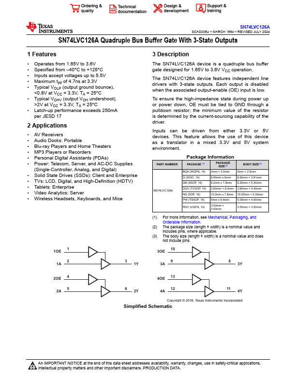
The SN74LVC126A device is a quadruple bus buffer gate designed for 1.65V to 3.6V VCC operation.

Key Features

  • Operates from 1.65V to 3.6V.
  • Specified from.
  • 40°C to +125°C.
  • Inputs accept voltages up to 5.5V.
  • Maximum tpd of 4.7ns at 3.3V.
  • Typical VOLP (output ground bounce), 2V at VCC = 3.3V, TA = 25°C.
  • Latch-up performance exceeds 250mA per JESD 17 2.

📥 Download Datasheet

Full PDF Text Transcription (Reference)

The following content is an automatically extracted verbatim text from the original manufacturer datasheet and is provided for reference purposes only.

View original datasheet text
SN74LVC126A SCAS339U – MARCH 1994 – REVISED JULY 2024 SN74LVC126A Quadruple Bus Buffer Gate With 3-State Outputs 1 Features • Operates from 1.65V to 3.6V • Specified from –40°C to +125°C • Inputs accept voltages up to 5.5V • Maximum tpd of 4.7ns at 3.3V • Typical VOLP (output ground bounce), <0.8V at VCC = 3.3V, TA = 25°C • Typical VOHV (output VOH undershoot), >2V at VCC = 3.