Datasheet Details
| Part number | SN74LVC1G125-Q1 |
|---|---|
| Manufacturer | Texas Instruments |
| File Size | 1.67 MB |
| Description | Single Bus Buffer Gate |
| Datasheet |
 SN74LVC1G125-Q1 Datasheet SN74LVC1G125-Q1 Datasheet
|
|
|
| Part number | SN74LVC1G125-Q1 |
|---|---|
| Manufacturer | Texas Instruments |
| File Size | 1.67 MB |
| Description | Single Bus Buffer Gate |
| Datasheet |
SN74LVC1G125-Q1 Datasheet
|
|
|
|
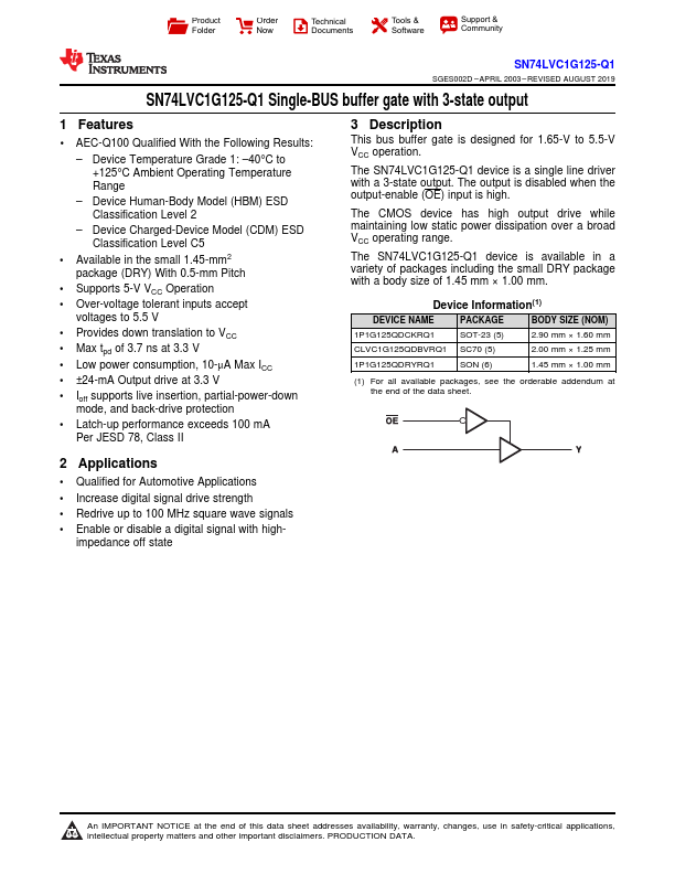
This bus buffer gate is designed for 1.65-V to 5.5-V VCC operation.
📁 Similar Datasheet