Datasheet4U Logo Datasheet4U.com

VDS8608A8A - Synchronous DRAM

This page provides the datasheet information for the VDS8608A8A, a member of the VDS8608A8A_A Synchronous DRAM family.

Datasheet Summary

Description

The VDS8608A8A are four-bank Synchronous DRAMs organized as 8,388,608 words x 8 bits x 4 banks.

Synchronous design allows precise cycle control with the use of system clock I/O transactions are possible on every clock cycle.

Features

  • JEDEC standard LVTTL 3.3V power supply.
  • MRS Cycle with address key programs -CAS Latency (2 & 3) -Burst Length (1,2,4,8,& full page) -Burst Type (sequential & Interleave).
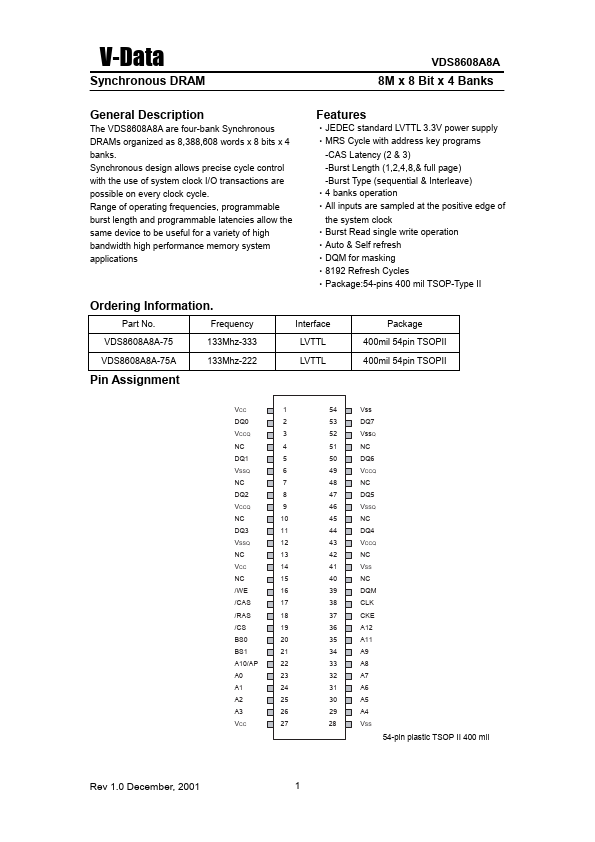
  • 4 banks operation.
  • All inputs are sampled at the positive edge of the system clock.
  • Burst Read single write operation.
  • Auto & Self refresh.
  • DQM for masking.
  • 8192 Refresh Cycles.
  • Package:54-pins 400 mil TSOP-Type II Ordering Information. Part No. Freque.

📥 Download Datasheet

Datasheet preview – VDS8608A8A

Datasheet Details

Part number VDS8608A8A
Manufacturer A-Data Technology
File Size 207.85 KB
Description Synchronous DRAM
Datasheet download datasheet VDS8608A8A Datasheet
Additional preview pages of the VDS8608A8A datasheet.
Other Datasheets by A-Data Technology

Full PDF Text Transcription

Click to expand full text
V-Data Synchronous DRAM VDS8608A8A 8M x 8 Bit x 4 Banks General Description The VDS8608A8A are four-bank Synchronous DRAMs organized as 8,388,608 words x 8 bits x 4 banks. Synchronous design allows precise cycle control with the use of system clock I/O transactions are possible on every clock cycle. Range of operating frequencies, programmable burst length and programmable latencies allow the same device to be useful for a variety of high bandwidth high performance memory system applications Features •JEDEC standard LVTTL 3.
Published: |