VDS4616A4A
VDS4616A4A is Synchronous DRAM manufactured by A-Data Technology.
- Part of the VDS4616A4A_A comparator family.
- Part of the VDS4616A4A_A comparator family.
Description
The VDS4616A4A are two-bank Synchronous DRAMs organized as 524,288 words x 16 bits x 2 banks, Synchronous design allows precise cycle control with the use of system clock I/O transactions are possible on every clock cycle. Range of operating frequencies, programmable burst length and programmable latencies allow the same device to be useful for a variety of high bandwidth high performance memory system applications
Features
- Single 3.3V +/- 0.3V power supply
- MRS Cycle with address key programs
-CAS Latency (2 & 3) -Burst Length (1,2,4,8, & full page) -Burst Type (sequential & Interleave)
- 2 banks operation
- All inputs are sampled at the positive edge of the system clock
- Burst Read single write operation
- Auto & Self refresh
- 4096 refresh cycle
- DQM for masking
- Package:50-pins 400 mil TSOP-Type II
Ordering Information.
Part No. VDS4616A4A-5 VDS4616A4A -6 VDS4616A4A -7
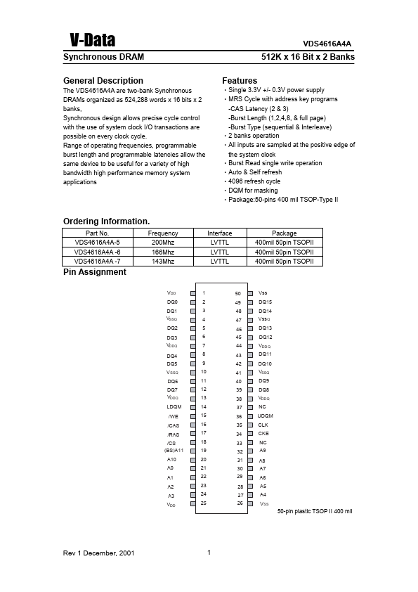
Pin...