IDCS3
IDCS3 is CMOS Gate Array manufactured by AMI.
Description
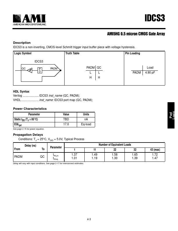
IDCS3 is a non-inverting, CMOS-level Schmitt trigger input buffer piece with voltage hysteresis.
Logic Symbol
Truth Table
Pin Loading
QC P PADM D
PADM QC LL HH
Load PADM 4.90 p F
HDL Syntax Verilog IDCS3 inst_name (QC, PADM); VHDL inst_name: IDCS3 port map (QC, PADM);
Power Characteristics
Parameter Static IDD (TJ = 85°C) EQLpd
See page 2-15 for power equation.
Value TBD 17.0
Units n A Eq-load
Propagation Delays Conditions: TJ = 25°C, VDD = 5.0V, Typical Process
Delay (ns) From
To
Parameter
PADM
QC t PLH t PHL
1.37 1.01
Delay will vary with input conditions. See page 2-17 for interconnect estimates.
Number of Equivalent Loads
11 22 32
1.49 1.58 1.65 1.19 1.30 1.39
43 (max)
1.72 1.47
Pad...