FEATURES
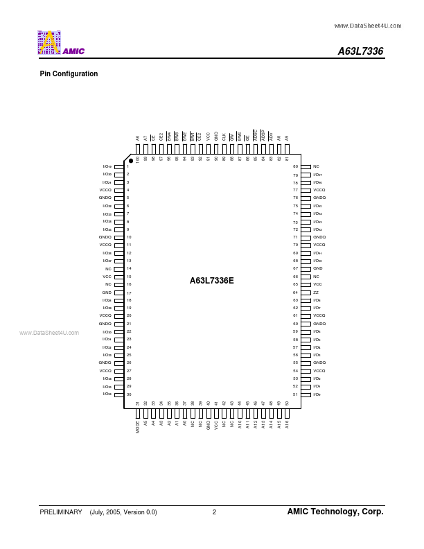
Fast access times: 2.6/2.8/3.2/3.5/3.8/4.2 ns (250/227/200/166/150/133 MHZ) Single +3.3V+10% or +3.3V-5% power supply Synchronous burst function Individual Byte Write control and Global Write Registered output for pipelined applications Three separate chip enables allow wide range of options for CE control, address pipelining Selectable BURST mode SLEEP mode (ZZ pin) provided Available in 100-pin LQFP package GENERAL DESCRIPTION
Synchronous inputs include all addresses (A0 A16), all data inputs (I/O1 - I/O36), active LOW chip enable ( CE ), two additional chip enables (CE2, CE2 ), burst control inputs ( ADSC , ADSP , ADV ), byte write enables ( BWE , BW1 , BW2 , BW3 , BW4 ) and Global Write ( GW ). Asynchronous inputs include output enable ( OE ), clock (CLK), BURST mode (MODE) and SLEEP mode (ZZ). Burst operations can be initiated with either the address status processor ( ADSP ) or address status controller ( ADSC ) input pin. Subsequent burst sequence burst addresses can be internally generated by the A63L7336 and controlled by the burst advance ( ADV ) pin. AMIC Technology