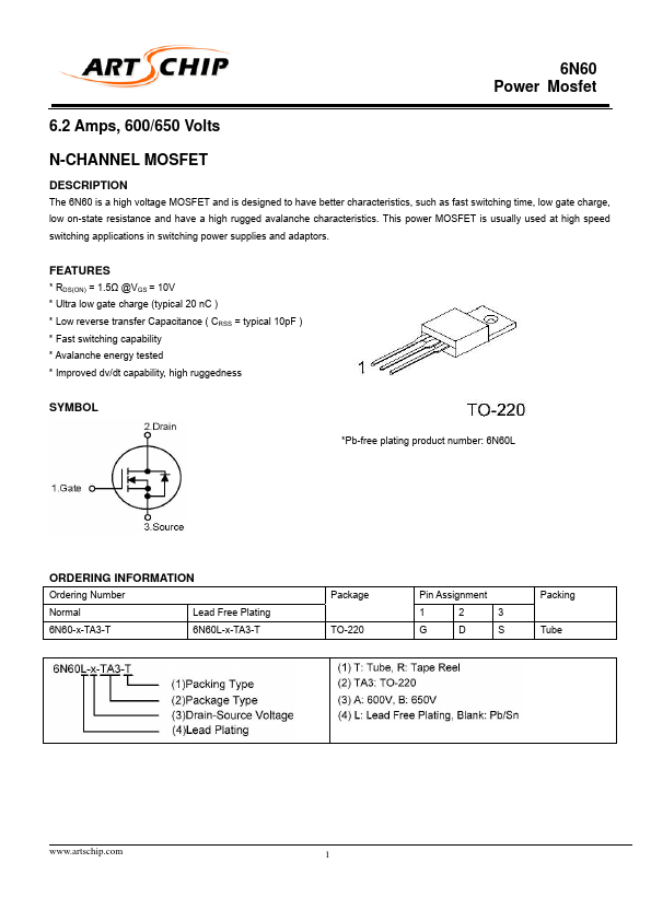
DESCRIPTION
FEATURES
* RDS(ON) = 1.5Ω @VGS = 10V * Ultra low gate charge (typical 20 nC ) * Low reverse transfer Capacitance ( CRSS = typical 10pF ) * Fast switching capability * Avalanche energy tested * Improved dv/dt capability, high ruggedness SYMBOL *Pb-free plating product number: 6N60L ORDERING INFORMATION Ordering Number Normal Lead Free Plating 6N60-x-TA3-T 6N60L-x-TA3-T Package TO-220 Pin Assignment 12 GD 3 S Packing Tube 1 6N60 Power Mosfet ABSOLUTE MAXIMUM RATINGS
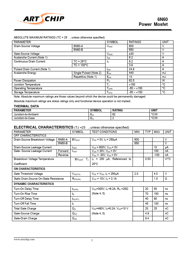
(TC = 25 , unless otherwise specified) PARAMETER SYMBOL RATINGS Drain-Source Voltage 6N60-A 6N60-B VDSS 600 650 Gate-Source Voltage VGSS ±30 Avalanche Current (Note 1) Continuous Drain Current TC = 25°C IAR 6.2 ID 6.2 TC = 100°C 3.9 Pulsed Drain Current (Note 1) Avalanche Energy Single Pulsed (Note 2) IDM EAS 24.8 440 Repetitive (Note 1) EAR 13 Power Dissipation Junction Temperature PD 62.5 TJ +150 Operating Temperature TOPR -55 ~ +150 Storage Temperature TSTG -55 ~ +150 Note: Absolute maximum ratings are those values beyond which the device could be permanently damaged. ART CHIP