ARTS CHIP 2N7002L
Small signal MOSFET
| Part No. | 2N7002L |
|---|---|
| Datasheet | 2N7002L Download |
| Manufacturer |  ARTS CHIP |
| Description | Small signal MOSFET |
| Buy | Stock & Price |
FEATURES
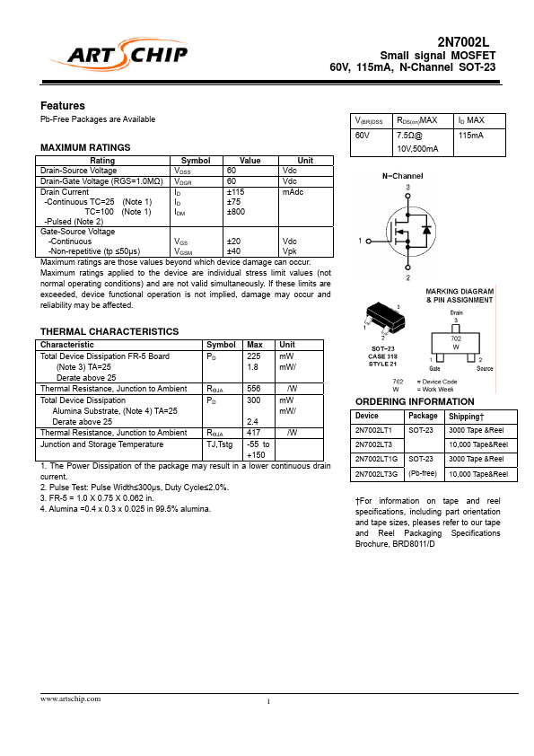
Pb-Free Packages are AvailableMAXIMUM RATINGS
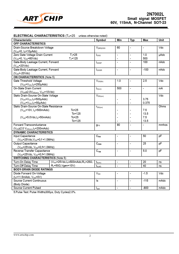
Rating Symbol Value Unit Drain-Source Voltage VDSS Drain-Gate Voltage (RGS=1.0MΩ) VDGR 60 60 Vdc Vdc Drain Current -Continuous TC=25 TC=100 -Pulsed (Note 2) (Note 1) (Note 1) ID ID IDM ±115 ±75 ±800 mAdc Gate-Source Voltage -Continuous -Non-repetitive (tp ≤50µs) VGS VGSM ±20 ±40 Vdc Vpk Maximum ratings are those values beyond which device damage can occur. Maximum ratings applied to the device are individual stress limit values (not normal operating conditions) and are not valid simultaneously. If these limits are exceeded, device functional operation is not implied, damage may occur and reliability may be affected. THERMAL CHARACTERISTICS Characteristic Symbol Max Unit Total Device Dissipation FR-5 Board (Note 3) TA=25 PD 225 mW 1.8 mW/ Derate above 25 Thermal Resistance, Junction to Ambient Total Device Dissipation Alumina Substrate, (Note 4) TA=25 RӨJA PD 556 /W 300 mW mW/ Derate above 25 2.4 Thermal Resistance, Junction to Ambient RӨJA 417 /W Junction and Storage Temperature TJ,Tstg -55 to +150 1.