AW5105DNR
AW5105DNR is BDS/GPS/GNSS INTEGRATED FRONT-END manufactured by AWINIC.
FEATURES
GENERAL DESCRIPTION l
- Low Noise Figure: 1.7d B;
- High power gain: 17d B typical @ 1.575 GHz
- Low current consumption: 6.9m A
- RF input/output impedance 50ohm
- Supply voltage: 1.5V-3.6V
- Operation frequency range: 1550MHz-1615MHz
The AW5105 is a Front-End Module (FEM) with a a fully integrated Low-Noise Amplifier and Pre-Filter for BDS/GPS/GNSS. The AW5105 requires no i external capacitor/inductor, reduces assembly t plexity and the PCB area, enabling a n cost-effective solution.
- Small DFN (6-pin, 1.5mm x 1.0 mm) package
- 3k V HBM ESD protection (including RFIN and
RFOUT pin)
- High Out-Of-Band jammer rejection at
Cellular/PCS/WLAN bands
- Fully-integrated module without any ponent at input/output side
The AW5105 achieves low noise figure, high gain, excellent linearity and high Out-Of-Band rejection. e All these feature make AW5105 an excellent choice for GNSS LNA as it improves sensitivity with low noise figure and high gain, provides better d immunity against out-of-band jammer signals with i high linearity, and reduces filtering requirement of f preceding stage and hence reduces the overall ncost of the GNSS receiver.
APPLICATIONS
- Small phones, Feature
Phones; o The AW5105 is provided in a pact 1.5mm x 1.0mm, 6-pin DFN package.
- Tablet PCs;
- Personal Navigation Devices;
- -
- ic plete GPS/BDS chipset modules;
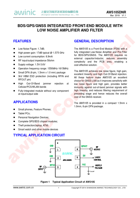
Theft protection(laptop, ATM) Smart watch and other mobile devices in TYPICAL APPLICATION CIRCUIT GND aw
1 GND
RFIN 3
INPUT
RFOUT 6
RF OUTPUT
EN 5
LOGIC CONTROL
VCC 4
SUPPLY VOLTAGE
C1=1n F
.awinic..cn
Figure 1 Typical Application Circuit of AW5105
Copyright © 2014 SHANGHAI AWINIC TECHNOLOGY CO., LTD
PIN CONFIGURATION AND TOP...