Datasheet4U Logo Datasheet4U.com

AP0904GYT-HF Datasheet N-CHANNEL ENHANCEMENT MODE POWER MOSFET

Manufacturer: Advanced Power Electronics Corp

General Description

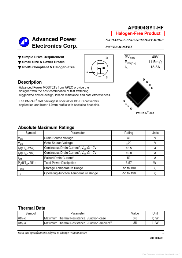
Advanced Power MOSFETs from APEC provide the designer with the best combination of fast switching, ruggedized device design, low on-resistance and cost-effectiveness.

The PMPAK® 3x3 package is special for DC-DC converters application and lower 1.0mm profile with backside heat sink.

S S D D D S G PMPAK ® 3x3 Absolute Maximum Ratings Symbol VDS VGS ID@TA=25℃ ID@TA=70℃ IDM PD@TA=25℃ TSTG TJ Parameter Drain-Source Voltage Gate-Source Voltage Continuous Drain Current , VGS @ 10V Continuous Drain Current , VGS @ 10V Pulsed Drain Current 1 3 3 Rating 40 +20 13.5 10.8 50 3.57 -55 to 150 -55 to 150 Units V V A A A W ℃ ℃ Total Power Dissipation Storage Temperature Range Operating Junction Temperature Range Thermal Data Symbol Rthj-c Rthj-a Parameter Maximum Thermal Resistance, Junction-case Maximum Thermal Resistance, Junction-ambient 3 Value 3.6 35 Unit ℃/W ℃/W 1 201104281 Data and specifications subject to change without notice Free Datasheet http://www.datasheet4u.com/ AP0904GYT-HF Electrical Characteristics@Tj=25oC(unless otherwise specified) Symbol BVDSS RDS(ON) VGS(th) gfs IDSS IGSS Qg Qgs Qgd td(on) tr td(off) tf Ciss Coss Crss Rg Parameter Drain-Source Breakdown Voltage Static Drain-Source On-Resistance Gate Threshold Voltage Forward Transconductance Drain-Source Leakage Current Gate-Source Leakage Total Gate Charge Gate-Source Charge Gate-Drain ("Miller") Charge Turn-on Delay Time Rise Time Turn-off Delay Time Fall Time Input Capacitance Output Capacitance Reverse Transfer Capacitance Gate Resistance 2 Test Conditions VGS=0V, ID=250uA VGS=10V, ID=13A VGS=4.5V, ID=8A VDS=VGS, ID=250uA VDS=10V, ID=13A VDS=32V, VGS=0V VGS=+20V, VDS=0V ID=13A VDS=20V VGS=4.5V VDS=20V ID=1A RG=3.3Ω VGS=10V VGS=0V VDS=15V f=

Overview

AP0904GYT-HF Halogen-Free Product Advanced Power Electronics Corp.

▼ Simple Drive Requirement ▼ Small Size & Lower Profile ▼ RoHS Compliant & Halogen-Free G N-CHANNEL ENHANCEMENT MODE POWER MOSFET D BVDSS RDS(ON) ID D 40V 11.5mΩ 13.