Datasheet Details
| Part number | AP1RC03GMT-HF |
|---|---|
| Manufacturer | Advanced Power Electronics Corp |
| File Size | 54.27 KB |
| Description | N-channel Enhancement mode Power MOSFET |
| Datasheet | AP1RC03GMT-HF-AdvancedPowerElectronics.pdf |
|
|
|
Overview: AP1RC03GMT-HF Halogen-Free Product Advanced Power Electronics Corp. 
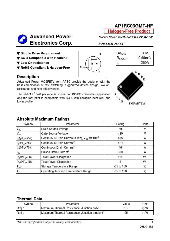
▼ Simple Drive Requirement ▼ SO-8 patible with Heatsink ▼ Low On-resistance ▼ RoHS pliant & Halogen-Free G N-CHANNEL ENHANCEMENT MODE POWER MOSFET D BVDSS RDS(ON) ID D 30V 0.
| Part number | AP1RC03GMT-HF |
|---|---|
| Manufacturer | Advanced Power Electronics Corp |
| File Size | 54.27 KB |
| Description | N-channel Enhancement mode Power MOSFET |
| Datasheet | AP1RC03GMT-HF-AdvancedPowerElectronics.pdf |
|
|
|
Advanced Power MOSFETs from APEC provide the designer with the best bination of fast switching, ruggedized device design, low onresistance and cost-effectiveness.
The PMPAK ® 5x6 package is special for DC-DC converters application and the foot print is patible with SO-8 with backside heat sink and lower profile.
S S D D D S G PMPAK ® 5x6 Absolute Maximum Ratings Symbol VDS VGS ID@TC=25℃ ID@TA=25℃ ID@TA=70℃ IDM PD@TC=25℃ PD@TA=25℃ TSTG TJ Parameter Drain-Source Voltage Gate-Source Voltage Continuous Drain Current (Chip), VGS @ 10V Continuous Drain Current Continuous Drain Current Pulsed Drain Current 1 3 3 4 Rating 30 +20 260 57.6 46 300 104 5 -55 to 150 -55 to 150 Units V V A A A A W W ℃ ℃ Total Power Dissipation Total Power Dissipation Storage Temperature Range Operating Junction Temperature Range Thermal Data Symbol Rthj-c Rthj-a Parameter Maximum Thermal Resistance, Junction-case Maximum Thermal Resistance, Junction-ambient 3 Value 1.2 25 Unit ℃/W ℃/W 1 201304102 Data and specifications subject to change without notice AP1RC03GMT-HF Electrical Characteristics@Tj=25oC(unless otherwise specified) Symbol BVDSS RDS(ON) VGS(th) gfs IDSS IGSS Qg Qgs Qgd td(on) tr td(off) tf Ciss Coss Crss Rg Parameter Drain-Source Breakdown Voltage Static Drain-Source On-Resistance Gate Threshold Voltage Forward Transconductance Drain-Source Leakage Current Gate-Source Leakage Total Gate Charge Gate-Source Charge Gate-Drain ("Miller") Charge Turn-on Delay Time Rise Time Turn-off Delay Time Fall Time Input Capacitance Output Capacitance Reverse Transfer Capacitance Gate Resistance 2 Test Conditions VGS=0V, ID=250uA VGS=10V, ID=25A VGS=5V, ID=25A VDS=VGS, ID=250uA VDS=5V, ID=25A VDS=24V, VGS=0V V
| Part Number | Description |
|---|---|
| AP1RC03GMT-HF-3 | N-channel Enhancement mode Power MOSFET |
| AP1R803GMT-HF | N-channel Enhancement mode Power MOSFET |
| AP1R803GMT-HF-3 | N-channel Enhancement mode Power MOSFET |
| AP1RA03GMT-HF | N-channel Enhancement mode Power MOSFET |
| AP1RA03GMT-HF-3 | N-channel Enhancement mode Power MOSFET |
| AP1001BSQ | N-CHANNEL ENHANCEMENT MODE POWER MOSFET |
| AP1001BSQ-3 | N-CHANNEL ENHANCEMENT MODE POWER MOSFET |
| AP1002BMX-3 | N-CHANNEL ENHANCEMENT MODE POWER MOSFET |
| AP1003BMP-3 | N-CHANNEL ENHANCEMENT MODE POWER MOSFET |
| AP1003BST | N-CHANNEL ENHANCEMENT MODE POWER MOSFET |