Datasheet Summary
30 P-Channel Enhancement-Mode MOSFET
VDS= -30V RDS(ON), Vgs@-10V, Ids@-9.1A = 21m RDS(ON), Vgs@-4.5V, Ids@-6.9A = 35m
Advanced trench process technology High Density Cell Design For Ultra Low On-Resistance
Preliminary Data Sheet
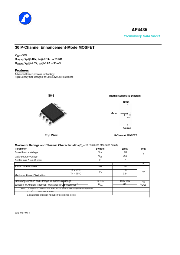
S0-8
Internal Schematic Diagram Drain
Gate
Top View
Source P-Channel MOSFET
Maximum Ratings and Thermal Characteristics (TA = 25 oC unless otherwise noted)
Parameter
Symbol
Drain-Source Voltage
Gate-Source Voltage Continuous Drain Current
VGS ID
Limit -30
±20 -7
Pulsed Drain Current 1) Maximum Power Dissipation
TA = 25oC TA = 75oC
IDM PD
-50 1.5 0.9
Operating Junction and Storage Temperature Range Junction-to-Ambient Thermal Resistance...