AP4959GM
AP4959GM is P-CHANNEL ENHANCEMENT MODE POWER MOSFET manufactured by Advanced Power Electronics Corp.
..
Pb Free Plating Product
Advanced Power Electronics Corp.
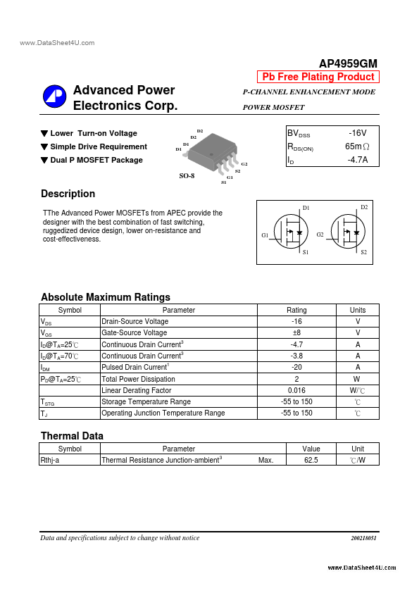
▼ Lower Turn-on Voltage ▼ Simple Drive Requirement ▼ Dual P MOSFET Package
SO-8
S1 S2 G1 D1 D1 D2 D2
P-CHANNEL ENHANCEMENT MODE POWER MOSFET
BVDSS RDS(ON)
G2
-16V 65mΩ -4.7A
Description
TThe Advanced Power MOSFETs from APEC provide the designer with the best bination of fast switching, ruggedized device design, lower on-resistance and cost-effectiveness.
D1 D2
G1 S1
G2...