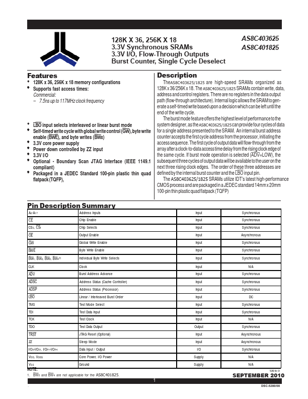
AS8C401825
AS8C401825 is 3.3V Synchronous SRAMs manufactured by Alliance Semiconductor.
- Part of the AS8C403625 comparator family.
- Part of the AS8C403625 comparator family.
128K X 36, 256K X 18 3.3V Synchronous SRAMs 3.3V I/O, Flow-Through Outputs Burst Counter, Single Cycle Deselect Features
- -
AS8C403625 AS8C401825
Description
TheAS8C403625/1825 are high-speed SRAMs organized as 128K x 36/256K x 18. The AS8C403625/1825 SRAMs contain write, data, address and control registers. There are no registers in the data output path (flow-through architecture). Internal logic allows the SRAM to generate a self-timed write based upon a decision which can be left until the end of the write cycle. The burst mode feature offers the highest level of performance to the system designer, as the AS8C403625/1825 can provide four cycles of data for a single address...