Datasheet Details
| Part number | AO4422 |
|---|---|
| Manufacturer | Alpha & Omega Semiconductors |
| File Size | 227.65 KB |
| Description | N-Channel MOSFET |
| Datasheet | AO4422_ETC.pdf |
|
|
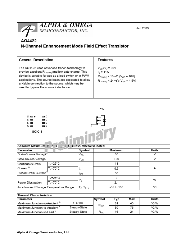
Overview: Jan 2003 AO4422 N-Channel Enhancement Mode Field Effect Transistor.
| Part number | AO4422 |
|---|---|
| Manufacturer | Alpha & Omega Semiconductors |
| File Size | 227.65 KB |
| Description | N-Channel MOSFET |
| Datasheet | AO4422_ETC.pdf |
|
|
|
The AO4422 uses advanced trench technology to provide excellent RDS(ON) and low gate charge.
This device is suitable for use as a load switch or in PWM applications.
The source leads are separated to allow a Kelvin connection to the source, which may be used to bypass the source inductance.
| Part Number | Description |
|---|---|
| AO4422A | N-Channel FET |
| AO4420 | 30V N-Channel MOSFET |
| AO4420A | 30V N-Channel MOSFET |
| AO4420L | N-Channel FET |
| AO4421 | 60V P-Channel MOSFET |
| AO4423 | 30V P-Channel MOSFET |
| AO4423L | 30V P-Channel MOSFET |
| AO4425 | 38V P-Channel MOSFET |
| AO4427 | P-Channel FET |
| AO4429 | P-Channel FET |