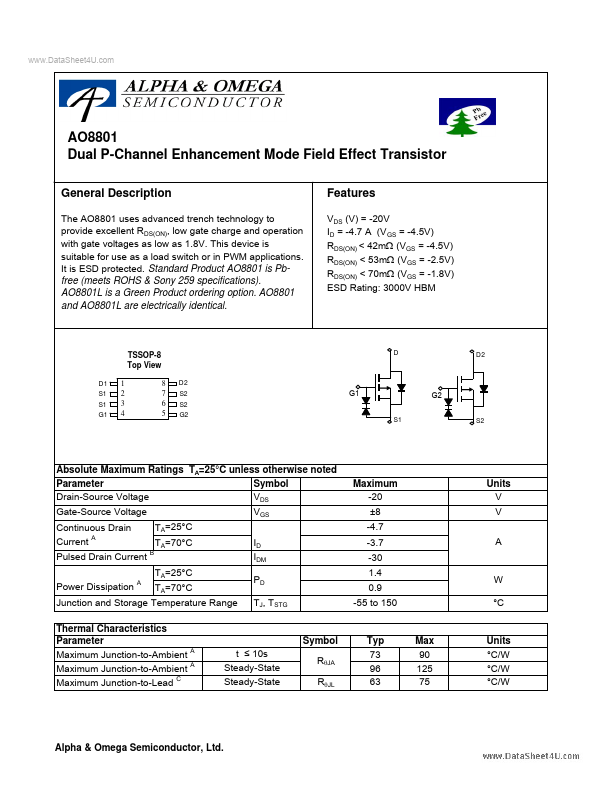
Datasheet4U Logo Datasheet4U.com

AO8801 - Dual P-Channel Enhancement Mode Field Effect Transistor

General Description

The AO8801 uses advanced trench technology to provide excellent RDS(ON), low gate charge and operation with gate voltages as low as 1.8V.

This device is suitable for use as a load switch or in PWM applications.

It is ESD protected.

Key Features

  • VDS (V) = -20V ID = -4.7 A (V GS = -4.5V) RDS(ON) < 42mΩ (VGS = -4.5V) RDS(ON) < 53mΩ (VGS = -2.5V) RDS(ON) < 70mΩ (VGS = -1.8V) ESD Rating: 3000V HBM TSSOP-8 Top View D1 S1 S1 G1 1 2 3 4 8 7 6 5 D2 S2 S2 G2 G1 D D2 G2 S1 S2 Absolute Maximum Ratings TA=25°C unless otherwise noted Parameter Symbol VDS Drain-Source Voltage VGS Gate-Source Voltage Continuous Drain Current A Pulsed Drain Current Power Dissipation A B Maximum -20 ±8 -4.7 -3.7 -30 1.4 0.9 -55 to 150 Units V V A TA=25°C TA=70°C.

📥 Download Datasheet

Full PDF Text Transcription (Reference)

The following content is an automatically extracted verbatim text from the original manufacturer datasheet and is provided for reference purposes only.

View original datasheet text
www.DataSheet4U.com AO8801 Dual P-Channel Enhancement Mode Field Effect Transistor General Description The AO8801 uses advanced trench technology to provide excellent RDS(ON), low gate charge and operation with gate voltages as low as 1.8V. This device is suitable for use as a load switch or in PWM applications. It is ESD protected. Standard Product AO8801 is Pbfree (meets ROHS & Sony 259 specifications). AO8801L is a Green Product ordering option. AO8801 and AO8801L are electrically identical. Features VDS (V) = -20V ID = -4.7 A (V GS = -4.5V) RDS(ON) < 42mΩ (VGS = -4.5V) RDS(ON) < 53mΩ (VGS = -2.5V) RDS(ON) < 70mΩ (VGS = -1.