Datasheet Details
| Part number | AOT11N60L |
|---|---|
| Manufacturer | Alpha & Omega Semiconductors |
| File Size | 457.21 KB |
| Description | 11A N-Channel MOSFET |
| Datasheet | AOT11N60L-AlphaOmegaSemiconductors.pdf |
|
|
Overview: AOT11N60L/AOTF11N60L/AOTF11N60 600V,11A N-Channel MOSFET General.
| Part number | AOT11N60L |
|---|---|
| Manufacturer | Alpha & Omega Semiconductors |
| File Size | 457.21 KB |
| Description | 11A N-Channel MOSFET |
| Datasheet | AOT11N60L-AlphaOmegaSemiconductors.pdf |
|
|
|
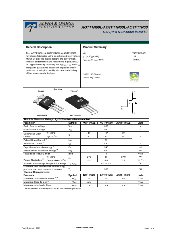
Product Summary The AOT11N60L & AOTF11N60L & AOTF11N60 have been fabricated using an advanced high voltage MOSFET process that is designed to deliver high levels of performance and robustness in popular ACDC applications.By providing low RDS(on), Ciss and Crss along with guaranteed avalanche capability these parts can be adopted quickly into new and existing offline power supply designs.
VDS ID (at VGS=10V) RDS(ON) (at VGS=10V) 100% UIS Tested 100% Rg Tested TO-220 D Top View TO-220F 700V@150℃ 11A < 0.65W D AOT11N60L S D G AOTF11N60(L) S GD Absolute Maximum Ratings TA=25°C unless otherwise noted Parameter Symbol AOT11N60L Drain-Source Voltage VDS Gate-Source Voltage VGS Continuous Drain Current TC=25°C TC=100°C ID 11 8 Pulsed Drain Current C IDM Avalanche Current C IAR Repetitive avalanche energy C EAR Single plused avalanche energy G EAS Peak diode recovery dv/dt dv/dt Power Dissipation B TC=25°C Derate above 25oC PD 272 2.2 Junction and Storage Temperature Range Maximum lead temperature for soldering purpose, 1/8" from case for 5 seconds Thermal Characteristics TJ, TSTG TL Parameter Maximum Junction-to-Ambient A,D Maximum Case-to-sink A Symbol RqJA RqCS AOT11N60L 65 0.5 Maximum Junction-to-Case RqJC 0.46 * Drain current limited by maximum junction temperature.
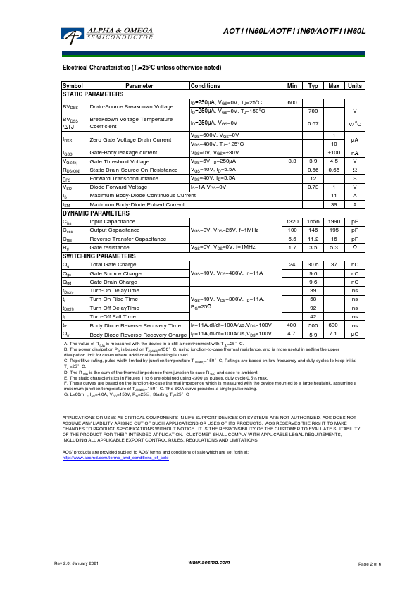
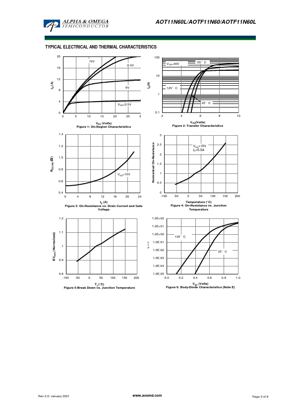
AOTF11N60 600 ±30 11* 8* 39 4.8 345 690 5 50 0.4 -55 to 150 300 AOTF11N60 65 -2.5 G S AOTF11N60L 11* 8* 37.9 0.3 AOTF11N60L 65 -3.3 Units V V A A mJ mJ V/ns W W/ oC °C °C Units °C/W °C/W °C/W Rev 2.0: January 2021 www.aosmd.com Page 1 of 6 AOT11N60L/AOTF11N60/AOTF11N60L Electrical Characteristics (TJ=25°C unless otherwise noted) Symbol Parameter Conditions Min Typ Max Units STATIC PARAMETERS BVDSS Drain-Source Breakdown Voltage ID=250μA, VGS=0V, TJ=25°C ID=250μA, VGS=0V, TJ=150°C BVDSS /∆TJ Breakdown Voltage Temperature Coefficient ID=250μA, VGS=0V IDSS Zero Gate Vo
Compare AOT11N60L distributor prices and check real-time stock availability from major suppliers. Prices and inventory may vary by region and order quantity.
| Brand Logo | Part Number | Description | Manufacturer |
|---|---|---|---|
| AOT11N60 | N-Channel MOSFET | INCHANGE |
| Part Number | Description |
|---|---|
| AOT11N60 | 11A N-Channel MOSFET |
| AOT11N70 | 11A N-Channel MOSFET |
| AOT1100L | 100V N-CHANNEL MOSFET |
| AOT11C60 | 11A N-Channel MOSFET |
| AOT11S60 | Power Transistor |
| AOT11S60L | Power Transistor |
| AOT11S65 | Power Transistor |
| AOT11S65L | 650V 11A Power Transistor |
| AOT10B60D | 10A IGBT |
| AOT10B65M1 | 10A Alpha IGBT |