Datasheet Details
| Part number | AOT20N25 |
|---|---|
| Manufacturer | Alpha & Omega Semiconductors |
| File Size | 337.44 KB |
| Description | 20A N-Channel MOSFET |
| Datasheet | AOT20N25-AlphaOmegaSemiconductors.pdf |
|
|
Overview: AOT20N25 250V,20A N-Channel MOSFET General.
| Part number | AOT20N25 |
|---|---|
| Manufacturer | Alpha & Omega Semiconductors |
| File Size | 337.44 KB |
| Description | 20A N-Channel MOSFET |
| Datasheet | AOT20N25-AlphaOmegaSemiconductors.pdf |
|
|
|
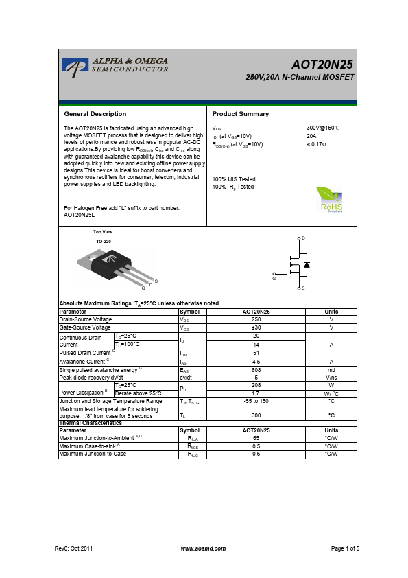
Product Summary The AOT20N25 is fabricated using an advanced high voltage MOSFET process that is designed to deliver high levels of performance and robustness in popular AC-DC applications.By providing low RDS(on), Ciss and Crss along with guaranteed avalanche capability this device can be adopted quickly into new and existing offline power supply designs.This device is ideal for boost converters and synchronous rectifiers for consumer, telecom, industrial power supplies and LED backlighting.
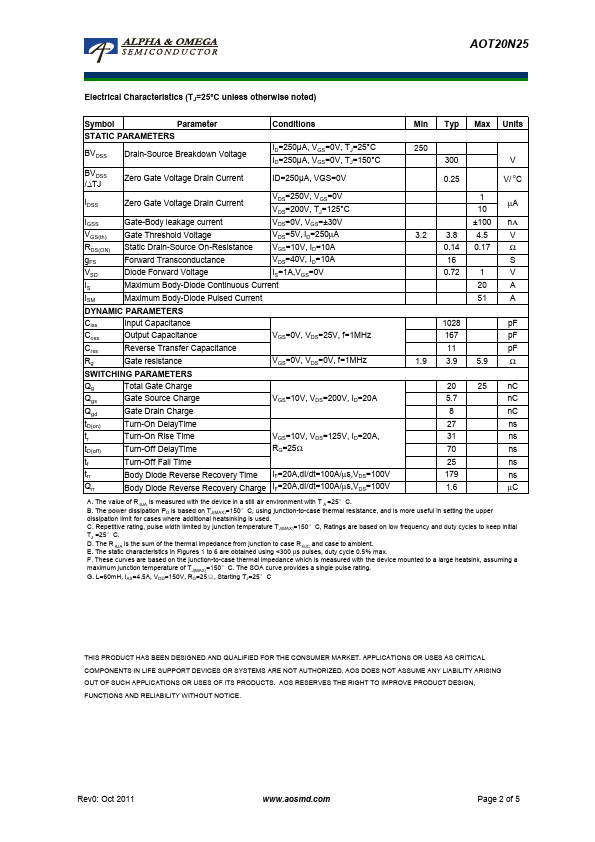
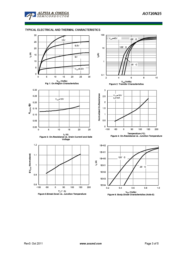
VDS ID (at VGS=10V) RDS(ON) (at VGS=10V) 100% UIS Tested 100% Rg Tested For Halogen Free add "L" suffix to part number: AOT20N25L Top View TO-220 300V@150℃ 20A < 0.17Ω D S D G Absolute Maximum Ratings TA=25°C unless otherwise noted Parameter Symbol Drain-Source Voltage VDS Gate-Source Voltage Continuous Drain TC=25°C Current TC=100°C Pulsed Drain Current C Avalanche Current C Single pulsed avalanche energy G Peak diode recovery dv/dt VGS ID IDM IAS EAS dv/dt TC=25°C Power Dissipation B Derate above 25oC PD Junction and Storage Temperature Range Maximum lead temperature for soldering purpose, 1/8" from case for 5 seconds Thermal Characteristics TJ, TSTG TL Parameter Maximum Junction-to-Ambient A,D Maximum Case-to-sink A Maximum Junction-to-Case Symbol RθJA RθCS RθJC G AOT20N25 250 ±30 20 14 51 4.5 608 5 208 1.7 -55 to 150 300 AOT20N25 65 0.5 0.6 S Units V V A A mJ V/ns W W/ oC °C °C Units °C/W °C/W °C/W Rev0: Oct 2011 www.aosmd.com Page 1 of 5 AOT20N25 Electrical Characteristics (TJ=25°C unless otherwise noted) Symbol Parameter Conditions Min Typ Max Units STATIC PARAMETERS BVDSS Drain-Source Breakdown Voltage ID=250µA, VGS=0V, TJ=25°C ID=250µA, VGS=0V, TJ=150°C BVDSS /∆TJ Zero Gate Voltage Drain Current ID=250µA, VGS=0V IDSS IGSS VGS(th) Zero Gate Voltage Drain Current Gate-Body leakage current Gate Threshold Voltage VDS=250V, VGS=0V VDS=200V, TJ=125°C VDS=0V, VGS=±30V VDS=5V,
| Brand Logo | Part Number | Description | Manufacturer |
|---|---|---|---|
| AOT20N25 | N-Channel MOSFET | INCHANGE | |
| AOT20N25 | Power MOSFET | VBsemi |
| Part Number | Description |
|---|---|
| AOT20N60 | 20A N-Channel MOSFET |
| AOT20B65M1 | IGBT |
| AOT20S60 | Power Transistor |
| AOT20S60L | Power Transistor |
| AOT210L | 30V N-Channel MOSFET |
| AOT2140L | 40V N-Channel MOSFET |
| AOT2142L | N-Channel MOSFET |
| AOT2144L | 40V N-Channel MOSFET |
| AOT2146L | 40V N-Channel MOSFET |
| AOT22N50 | 22A N-Channel MOSFET |