AON2260 Overview
Key Specifications
Package: DFN
Mount Type: Surface Mount
Max Operating Temp: 150 °C
Min Operating Temp: -55 °C
Description
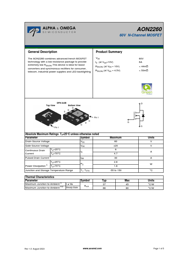
Product Summary The AON2260 combines advanced trench MOSFET technology with a low resistance package to provide extremely low RDS(ON).This device is ideal for boost converters and synchronous rectifiers for consumer, telecom, industrial power supplies and LED backlighting. VDS ID (at VGS=10V) RDS(ON) (at VGS = 10V) RDS(ON) (at VGS = 4.5V) 60V 6A < 44mW < 53mW DFN 2x2B Top View Bottom View D D S D S Pin 1 D D G G Pin 1 Parameter Symbol Drain-Source Voltage VDS Gate-Source Voltage VGS Continuous Drain Current TA=25°C TA=70°C ID Pulsed Drain Current C IDM TA=25°C Power Dissipation A TA=70°C PD Junction and Storage Temperature Range TJ, TSTG Maximum 60 ±20 6 4.7 30 2.8 1.8 -55 to 150 Parameter Symbol Typ Maximum Junction-to-Ambient A t ≤ 10s Maximum Junction-to-Ambient A D Steady-State RqJA 37 66 Max 45 80 D S Units V V A A W °C Units °C/W °C/W Rev 1.0: August 2023 Page 1 of 5 AON2260 Symbol Parameter Conditions Min Typ Max Units STATIC PARAMETERS BVDSS IDSS IGSS VGS(th) ID(ON) RDS(ON) gFS VSD IS Drain-Source Breakdown Voltage ID=250mA, VGS=0V 60 Zero Gate Voltage Drain Current VDS=60V, VGS=0V TJ=55°C Gate-Body leakage current VDS=0V, VGS=±20V Gate Threshold Voltage VDS=VGS,ID=250mA 1.5 On state drain current VGS=10V, VDS=5V 30 VGS=10V, ID=6A Static Drain-Source On-Resistance TJ=125°C VGS=4.5V, ID=4A Forward Transconductance VDS=5V, ID=6A Diode Forward Voltage IS=1A,VGS=0V Maximum Body-Diode Continuous Current V 1 5 mA ±100 nA 2 2.5 V A 36 44 61.5 75 mW 42 53 mW 21 S 0.75 1 V 3.5 A DYNAMIC PARAMETERS Ciss Input Capacitance Coss Output Capacitance Crss Reverse Transfer Capacitance Rg Gate resistance VGS=0V, VDS=30V, f=1MHz VGS=0V, VDS=0V, f=1MHz 4.