Datasheet4U Logo Datasheet4U.com

AON6572 Datasheet 30v N-channel MOSFET

Manufacturer: Alpha & Omega Semiconductors

Overview: AON6572 30V N-Channel AlphaMOS General.

General Description

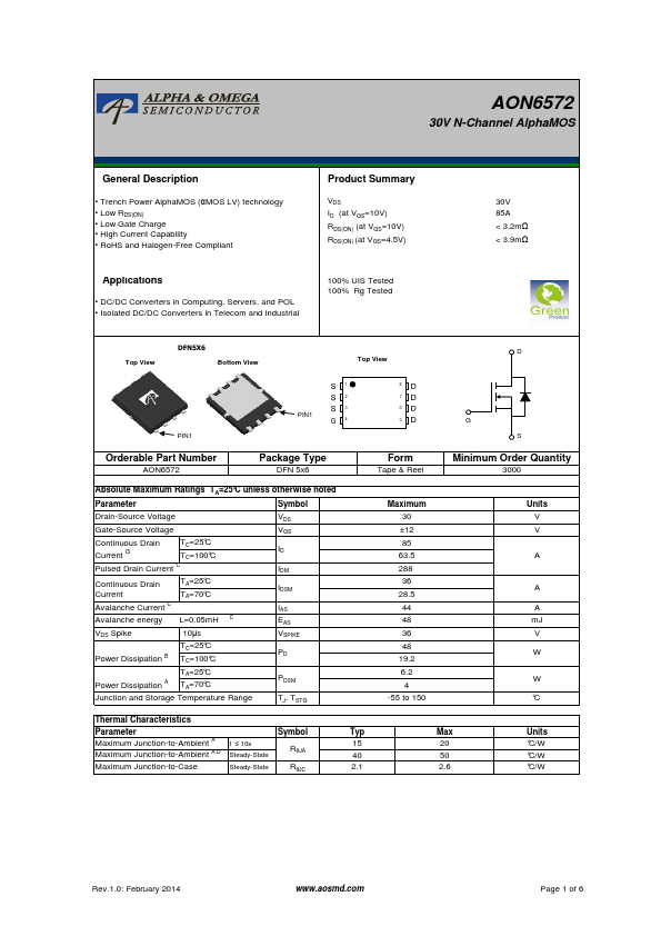
• Trench Power AlphaMOS (αMOS LV) technology • Low RDS(ON) • Low Gate Charge • High Current Capability • RoHS and Halogen-Free pliant Product Summary VDS ID (at VGS=10V) RDS(ON) (at VGS=10V) RDS(ON) (at VGS=4.5V) Applications • DC/DC Converters in puting, Servers, and POL • Isolated DC/DC Converters in Tele and Industrial 100% UIS Tested 100% Rg Tested 30V 85A < 3.2mΩ < 3.9mΩ DFN5X6 D Top View Bottom View Top View PIN1 1 8 2 7 3 6 PIN1 4 5 G S Orderable Part Number AON6572 Package Type DFN 5x6 Form Tape & Reel Minimum Order Quantity 3000 Absolute Maximum Ratings TA=25°C unless otherwise noted Parameter Symbol Drain-Source Voltage VDS Gate-Source Voltage VGS Continuous Drain Current G TC=25°C TC=100°C ID Pulsed Drain Current C IDM Continuous Drain Current TA=25°C TA=70°C IDSM Avalanche Current C IAS Avalanche energy L=0.05mH C EAS VDS Spike Power Dissipation B 10µs TC=25°C TC=100°C VSPIKE PD TA=25°C Power Dissipation A TA=70°C PDSM Junction and Storage Temperature Range TJ, TSTG Maximum 30 ±12 85 63.5 288 36 28.5 44 48 36 48 19.2 6.2 4 -55 to 150 Units V V A A A mJ V W W °C Thermal Characteristics Parameter Symbol Typ Maximum Junction-to-Ambient A t ≤ 10s Maximum Junction-to-Ambient A D Steady-State RθJA 15 40 Maximum Junction-to-Case Steady-State RθJC 2.1 Max 20 50 2.6 Units °C/W °C/W °C/W Rev.1.0: February 2014 .aosmd.

Page 1 of 6 Electrical Characteristics (TJ=25°C unless otherwise noted) Symbol Parameter Conditions Min STATIC PARAMETERS BVDSS Drain-Source Breakdown Voltage ID=250µA, VGS=0V 30 IDSS Zero Gate Voltage Drain Current VDS=30V, VGS=0V TJ=55°C IGSS Gate-Body leakage current VDS=0V, VGS=±12V VGS(th) Gate Threshold Voltage VDS=VGS, ID=250µA 1.2 VGS=10V, ID=20A RDS(ON) Static Drain-Source On-Resistance TJ=125°C VGS=4.5V, ID=20A gFS Forward Transconductance VDS=5V, ID=20A VSD Diode Forward Voltage

AON6572 Distributor