AD9867
AD9867 is Broadband Modem Mixed-Signal Front End manufactured by Analog Devices.
FEATURES
Low cost, 3.3 V CMOS Mx FE® for broadband modems 10-bit digital-to-analog converter (DAC) 2×/4× interpolation filter 250 MSPS DAC update rate 10-bit, 75 MSPS ADC Low noise Rx PGA Dual channel muxed input 6 d B input overload attenuator
- 12 d B to +48 d B (without attenuator) Third-order programmable low-pass filter Flexible digital datapath interface Half-duplex and full-duplex operation Programmable delay Tx driver disable signal Various power-down/reduction modes Internal clock multiplier (PLL) 2 auxiliary programmable clock outputs 64-lead LFCSP
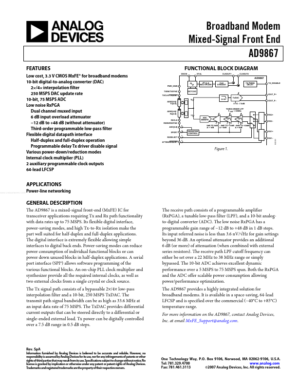
FUNCTIONAL BLOCK DIAGRAM
OSCIN XTAL CLKOUT1 CLKOUT2
PWR_DWN TXEN/TXSYNC TXCLK/TXQUIET ADIO[9:5]/ Tx[4:0] 10 2×/4× Tx DAC IOUT_P- 0 TO
- 7.5d B THIRD-ORDER LPF f- 3d B = 33MHz 10 RX2+ ADC 80MSPS
2-POLE LPF 1-POLE LPF
2M CLK MULTIPLIER DCTCXO
CLK SYN/DIST
TX PWDN DELAY
TX_DISABLE
IOUT_P+
ADIO[4:0]/ Rx[4:0] RXCLK RXEN/RXSYNC AGC[4:0] SPORT RXSELECT ATTEN/RXQUIET 5 4 1 1
RX2-
0d B TO 6d B
- 6d B TO +18d B
- 6d B TO +24d B Δ = 1d B Δ = 6d B Δ = 6d B REGISTER CONTROL RX1+ RX1-
Figure 1.
APPLICATIONS
..
Power-line networking
GENERAL DESCRIPTION
The AD9867 is a mixed-signal front-end (Mx FE) IC for transceiver applications requiring Tx and Rx path functionality with data rates up to 75 MSPS. Its flexible digital interface, power-saving modes, and high Tx-to-Rx isolation make the part well suited for half-duplex and full-duplex applications. The digital interface is extremely flexible allowing simple interfaces to digital back ends. Power-saving modes can reduce power consumption of individual functional blocks or can power down unused blocks in half-duplex applications. A serial port interface (SPI®) allows software programming of the various functional blocks. An on-chip PLL clock multiplier and synthesizer provide all the required internal clocks, as well as two external clocks from a single crystal or clock source. The Tx signal path consists of a bypassable 2×/4× low-pass interpolation filter and a 10-bit, 250 MSPS...