ADG1206L
ADG1206L is iCMOS Multiplexer manufactured by Analog Devices.
Data Sheet ADG1206L/ADG1207L
Low Capacitance, 16-Channel and 8-Channel i CMOS Multiplexers with 1.2 V and
1.8 V JEDEC Logic pliance
Features
FUNCTIONAL BLOCK DIAGRAMS
- <1 p C charge injection over full signal range
- 1.5 p F off capacitance
- 120 Ω on resistance
- Fully specified at ±15 V/+12 V
- VL supply for low logic-level patibility
- 1.8 V JEDEC standard pliant (JESD8-7A)
- 1.2 V JEDEC standard pliant (JESD8-12A.01)
- Rail-to-rail operation
- Break-before-make switching action
- 32-lead, 5 mm × 5 mm LFCSP
APPLICATIONS
- Audio and video routing
- Automatic test equipment
- Data acquisition systems
- Battery-powered systems
- Sample-and-hold systems
- munication systems
- FPGA and microcontroller systems
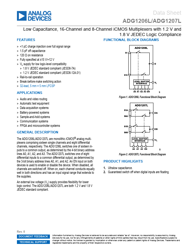
Figure 1. ADG1206L Functional Block Diagram
GENERAL DESCRIPTION
The ADG1206L/ADG1207L are monolithic i CMOS® analog multiplexers prising sixteen single channels and eight differential channels, respectively. The ADG1206L switches one of sixteen inputs to a mon output, as determined by the 4‑bit binary address lines A0, A1, A2, and A3. The ADG1207L switches one of eight differential inputs to a mon differential output, as determined by the 3-bit binary address lines A0, A1, and A2. An EN input on both devices is used to enable or disable the device. When disabled, all channels are switched off. When on, each channel conducts equally well in both directions and has an input signal range that extends to the supplies.
Figure 2. ADG1207L Functional Block Diagram
PRODUCT HIGHLIGHTS 1. Ultralow capacitance. 2. Guaranteed switch off when digital inputs are floating.
An external low voltage (VL) supply provides flexibility for lower logic control. The ADG1206L/ADG1207L are both 1.2 V and 1.8 V JEDEC standard pliant.
Rev. 0 DOCUMENT FEEDBACK TECHNICAL...