ADL8143
ADL8143 is Low Noise Amplifier manufactured by Analog Devices.
FEATURES
- Single positive supply (self biased) typical: 1.5 V and 35 m A
- RBIAS drain current adjustment pin
- Gain: 28.5 d B from 8 GHz to 10 GHz
- Noise figure: 1 d B from 8 GHz to 10 GHz
- Extended operating temperature range:
- 55°C to +125°C
- Internally matched and AC-coupled
- Ro HS-pliant, 2 mm × 2 mm, 8-lead LFCSP
APPLICATIONS
- Satellite munications
- Radar
- Telemunications
GENERAL DESCRIPTION
The ADL8143 is a low noise amplifier (LNA) that operates from 8 GHz to 14 GHz. The typical gain, noise figure, output power for 1 d B pression (OP1d B), and output third-order intercept (OIP3) are 28.5 d B, 1 d B, 7.5 d Bm, and 19.5 d Bm, respectively, from 8 GHz to 10 GHz. The nominal quiescent current (IDQ), which can be adjusted, is 35 m A from a 1.5 V supply voltage (VDD). The ADL8143 also features inputs and outputs that are AC-coupled and internally matched to 50 Ω.
The ADL8143 is housed in an Ro HS-pliant, 2 mm × 2 mm, 8-lead lead frame chip scale package [LFCSP] and is specified for operation from
- 55°C to +125°C.
Data Sheet ADL8143
8 GHz to 14 GHz, Low Noise Amplifier
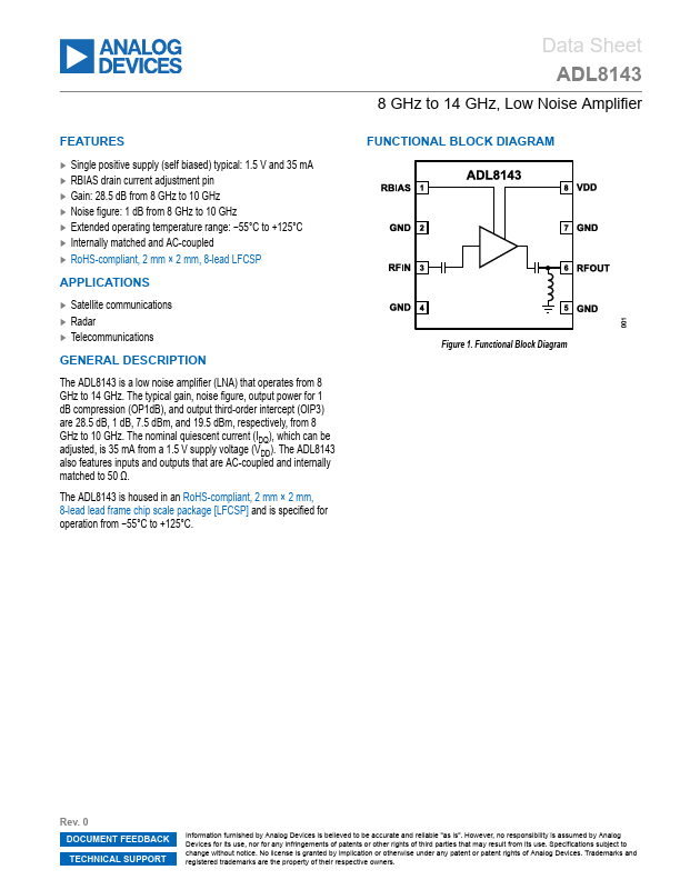
FUNCTIONAL BLOCK DIAGRAM
Figure 1. Functional Block Diagram
Rev. 0 DOCUMENT FEEDBACK TECHNICAL SUPPORT
Information furnished by Analog Devices is believed to be accurate and reliable "as is". However, no responsibility is assumed by Analog Devices for its use, nor for any infringements of patents or other rights of third parties that may result from its use. Specifications subject to change without notice. No license is granted by implication or otherwise under any patent or patent rights of Analog Devices. Trademarks and registered trademarks are the property of their respective owners.
Data Sheet
TABLE OF CONTENTS
Features
1 Applications 1 General Description
1 Functional Block Diagram 1...