ADM2481
ADM2481 is Isolated RS-485 Transceiver manufactured by Analog Devices.
FEATURES
- RS-485 transceiver with electrical data isolation
- plies with ANSI TIA/EIA-485-A and ISO 8482: 1987(E)
- 500 kbps data rate
- Slew rate-limited driver outputs
- Low power operation: 2.5 m A maximum
- Suitable for 5 V or 3.3 V operations (VDD1)
- High mon-mode transient immunity: >25 k V/μs
- True fail-safe receiver inputs
- Chatter-free power-up/power-down protection
- 256 nodes on bus
- Thermal shutdown protection
- Safety and regulatory approvals
- UL 1577
- VISO = 2500 V rms for 1 minute
- DIN EN IEC 60747-17 (VDE 0884-17)
- VIORM = 560 V peak
- Operating temperature range:
- 40°C to +85°C
APPLICATIONS
- Low power RS-485/RS-422 networks
- Isolated interfaces
- Building control networks
- Multipoint data transmission systems
GENERAL DESCRIPTION
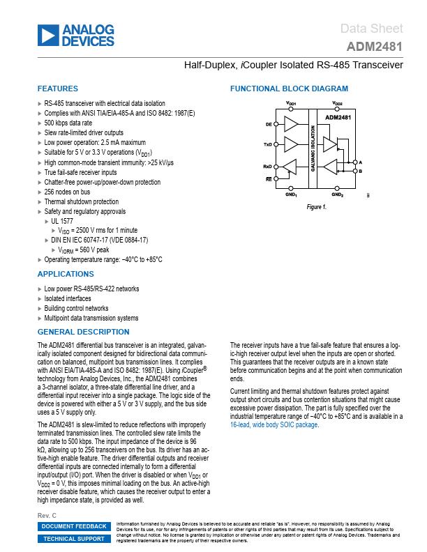
The ADM2481 differential bus transceiver is an integrated, galvanically isolated ponent designed for bidirectional data munication on balanced, multipoint bus transmission lines. It plies with ANSI EIA/TIA-485-A and ISO 8482: 1987(E). Using i Coupler® technology from Analog Devices, Inc., the ADM2481 bines a 3-channel isolator, a three-state differential line driver, and a differential input receiver into a single package. The logic side of the device is powered with either a 5 V or 3 V supply, and the bus side uses a 5 V supply only.
The ADM2481 is slew-limited to reduce reflections with improperly terminated transmission lines. The controlled slew rate limits the data rate to 500 kbps. The input impedance of the device is 96 kΩ, allowing up to 256 transceivers on the bus. Its driver has an active-high enable feature
. The driver differential outputs and receiver differential inputs are connected internally to form a differential input/output (I/O) port. When the driver is disabled or when VDD1 or VDD2 = 0 V, this imposes minimal loading on the bus. An active-high receiver disable feature
, which causes the receiver output to enter a high impedance state, is provided as well.
FUNCTIONAL BLOCK DIAGRAM
Figure 1.
The...