ADN4662
ADN4662 is LVDS Differential Line Receiver manufactured by Analog Devices.
FEATURES
±15 k V ESD protection on input pins 400 Mbps (200 MHz) switching rates Flow-through pinout simplifies PCB layout 2.5 ns maximum propagation delay 3.3 V power supply High impedance outputs on power-down Low power design: typically 3 m W (quiescent) Interoperable with existing 5 V LVDS drivers Accepts small swing (310 m V typical) differential signal levels Supports open, short, and terminated input fail-safe 0 V to
- 100 m V threshold region Conforms to TIA/EIA-644 LVDS standard Industrial operating temperature range:
- 40°C to +85°C Available in surface-mount (SOIC) package
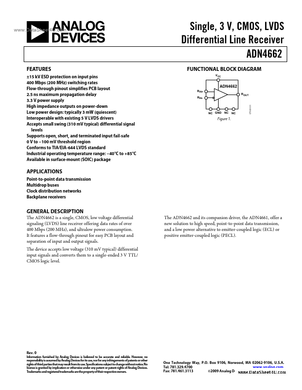
RIN+ RIN- ROUT
NC GND NC NC
Figure 1.
APPLICATIONS
Point-to-point data transmission Multidrop buses Clock distribution networks Backplane receivers
GENERAL DESCRIPTION
The ADN4662 is a single, CMOS, low voltage differential signaling (LVDS) line receiver offering data rates of over 400 Mbps (200 MHz), and ultralow power consumption. It features a flow-through pinout for easy PCB layout and separation of input and output signals. The device accepts low voltage (310 m V typical) differential input signals and converts them to a single-ended 3 V TTL/ CMOS logic level. The ADN4662 and its panion driver, the ADN4661, offer a new solution to high speed, point-to-point data transmission, and a low power alternative to emitter-coupled logic (ECL) or positive emitter-coupled logic (PECL).
Rev. 0
Information furnished by Analog Devices is believed to be accurate and reliable. However, no responsibility is assumed by Analog Devices for its use, nor for any infringements of patents or other rights of third parties that may result from its use. Specifications subject to change without notice. No license is granted by implication or otherwise under any patent or patent rights of Analog Devices. Trademarks and registered trademarks are the property of their respective owners.
One Technology Way, P.O. Box 9106, Norwood, MA 02062-9106, U.S.A. Tel: 781.329.4700 .analog. Fax: 781.461.3113 ©2009...