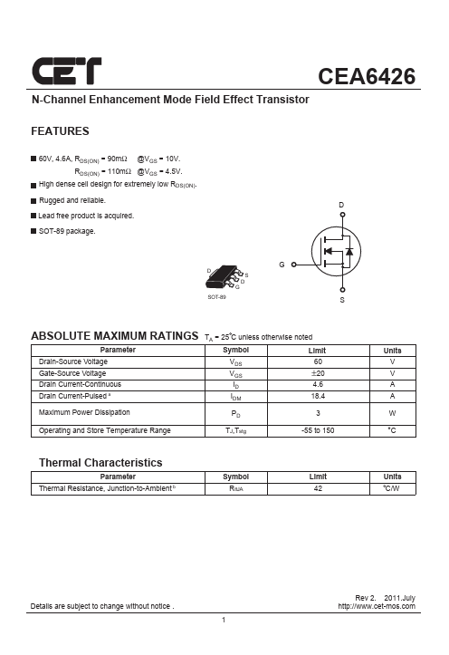
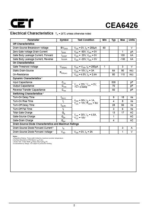
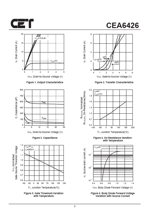
Click to expand full text
CEA6426
N-Channel Enhancement Mode Field Effect Transistor
FEATURES
60V, 4.6A, RDS(ON) = 90mΩ @VGS = 10V. RDS(ON) = 110mΩ @VGS = 4.5V.
High dense cell design for extremely low RDS(ON). Rugged and reliable. Lead free product is acquired. SOT-89 package.
D
D SOT-89
S D G
G
S
ABSOLUTE MAXIMUM RATINGS TA = 25 C unless otherwise noted
Parameter
Symbol
Limit
Drain-Source Voltage Gate-Source Voltage
VDS 60
VGS ±20
Drain Current-Continuous Drain Current-Pulsed a
ID 4.6 IDM 18.4
Maximum Power Dissipation
PD 3
Operating and Store Temperature Range
TJ,Tstg
-55 to 150
Thermal Characteristics
Parameter Thermal Resistance, Junction-to-Ambient b
Symbol RθJA
Limit 42
Units V V A A W C
Units C/W
Details are subject to change without notice .
1
Rev 2. 2011.July http://www.cet-mos.