CEA6861 Key Features
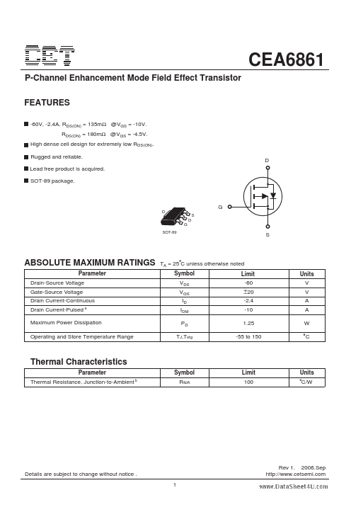
- 60V, -2.4A, RDS(ON) = 135mΩ @VGS = -10V. RDS(ON) = 180mΩ @VGS = -4.5V. High dense cell design for extremely low RDS(ON).
CEA6861 is P-Channel Enhancement Mode Field Effect Transistor manufactured by CET.
| Part Number | Description |
|---|---|
| CEA6200 | N-Channel MOSFET |
| CEA6426 | N-Channel MOSFET |
| CEA3252 | N-Channel MOSFET |
CEA6861 P-Channel Enhancement Mode Field Effect Transistor.