CED06N7
CED06N7 is N-Channel MOSFET manufactured by CET.
FEATURES
700V, 5A, RDS(ON) = 2Ω @VGS = 10V. Super high dense cell design for extremely low RDS(ON). High power and current handing capability. Lead-free plating ; Ro HS pliant. TO-251 & TO-252 package.
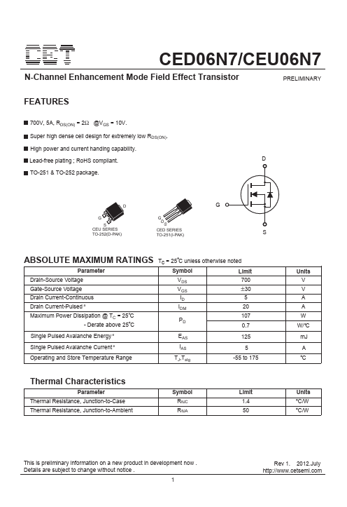
CEU SERIES TO-252(D-PAK)
G DS
CED SERIES TO-251(I-PAK)
ABSOLUTE MAXIMUM RATINGS Tc = 25 C unless otherwise noted
Parameter
Symbol
Limit
Drain-Source Voltage Gate-Source Voltage
VDS 700
VGS ±30
Drain Current-Continuous Drain Current-Pulsed a
ID 5 IDM 20
Maximum Power Dissipation @ TC = 25 C
- Derate above 25 C
107 0.7
Single Pulsed Avalanche Energy e
EAS 125
Single Pulsed Avalanche Current e
IAS 5
Operating and Store Temperature Range
TJ,Tstg
-55 to 175
Thermal Characteristics
Parameter Thermal Resistance, Junction-to-Case Thermal Resistance, Junction-to-Ambient
Symbol RθJC RθJA
Limit 1.4 50
Units V V A A W
W/ C m J A C
Units C/W C/W
This is preliminary...