Datasheet Summary
..net
Jul. 2002
Dual Enhancement Mode Field Effect Transistor ( N and P Channel)
Features
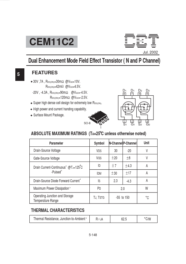
30V ,7A , RDS(ON)=30m Ω @VGS=10V. RDS(ON)=42mΩ @VGS=4.5V. -20V , -4.3A , RDS(ON)=90m Ω @VGS=-4.5V. RDS(ON)=120mΩ @VGS=-2.5V. Super high dense cell design for extremely low RDS(ON). High power and current handing capability. Surface Mount Package.
SO-8 1
1 2 3 4
D1
D1
D2
D2
S1
G1...