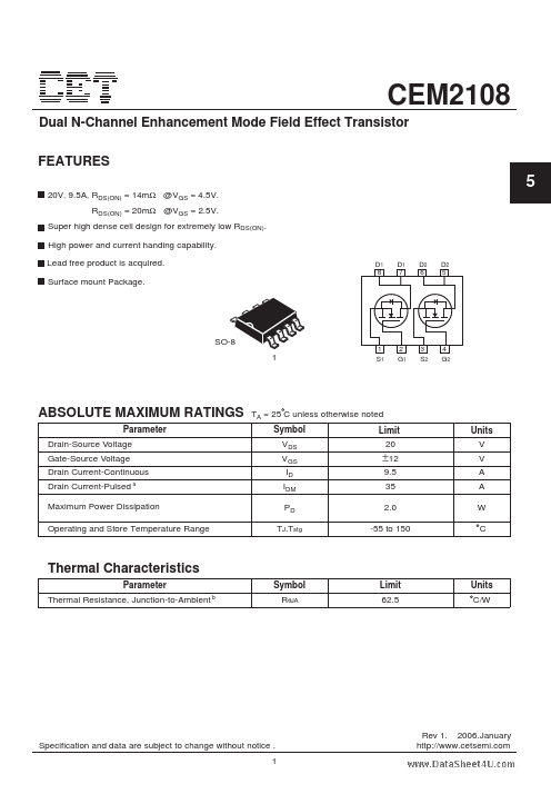
CEM2108 Description
CEM2108 Dual N-Channel Enhancement Mode Field Effect Transistor.
CEM2108 is Dual N-Channel Enhancement Mode Field Effect Transistor manufactured by CET.
| Part Number | Description |
|---|---|
| CEM2108E | Dual N-Channel MOSFET |
| CEM2133 | P-Channel Enhancement Mode Field Effect Transistor |
| CEM2163 | P-Channel MOSFET |
| CEM2182 | N-Channel MOSFET |
| CEM2187 | P-Channel Enhancement Mode Field Effect Transistor |
CEM2108 Dual N-Channel Enhancement Mode Field Effect Transistor.