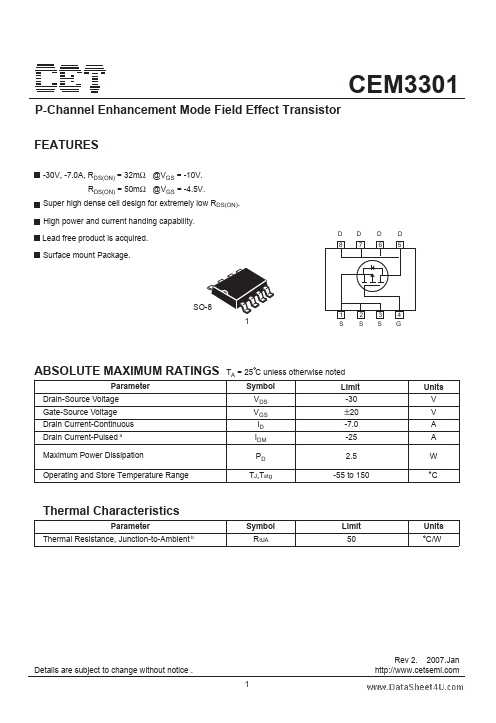
CEM3301 Key Features
- 30V, -7.0A, RDS(ON) = 32mΩ @VGS = -10V. RDS(ON) = 50mΩ @VGS = -4.5V. Super high dense cell design for extremely low RDS(
CEM3301 is P-Channel Enhancement Mode Field Effect Transistor manufactured by CET.
| Part Number | Description |
|---|---|
| CEM3307 | P-Channel Enhancement Mode Field Effect Transistor |
| CEM3317 | P-Channel Enhancement Mode Field Effect Transistor |
| CEM3053 | P-Channel MOSFET |
| CEM3060 | N-Channel Enhancement Mode Field Effect Transistor |
| CEM3082 | N-Channel Enhancement Mode Field Effect Transistor |
P-Channel Enhancement Mode Field Effect Transistor.