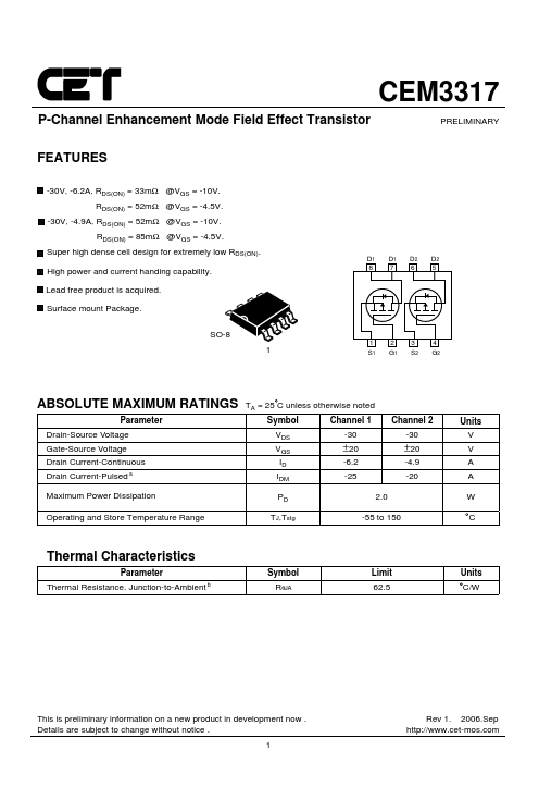
Datasheet4U Logo Datasheet4U.com

CEM3317 - P-Channel Enhancement Mode Field Effect Transistor

Key Features

  • -30V, -6.2A, RDS(ON) = 33mΩ @VGS = -10V. RDS(ON) = 52mΩ @VGS = -4.5V. -30V, -4.9A, RDS(ON) = 52mΩ @VGS = -10V. RDS(ON) = 85mΩ @VGS = -4.5V. Super high dense cell design for extremely low RDS(ON). High power and current handing capability. Lead free product is acquired. Surface mount Package. SO-8 1 D1 D1 D2 D2 876 5 123 4 S1 G1 S2 G2.

📥 Download Datasheet

Datasheet Details

Part number CEM3317
Manufacturer CET
File Size 426.23 KB
Description P-Channel Enhancement Mode Field Effect Transistor
Datasheet download datasheet CEM3317 Datasheet

Full PDF Text Transcription (Reference)

The following content is an automatically extracted verbatim text from the original manufacturer datasheet and is provided for reference purposes only.

View original datasheet text
CEM3317 P-Channel Enhancement Mode Field Effect Transistor PRELIMINARY FEATURES -30V, -6.2A, RDS(ON) = 33mΩ @VGS = -10V. RDS(ON) = 52mΩ @VGS = -4.5V. -30V, -4.9A, RDS(ON) = 52mΩ @VGS = -10V. RDS(ON) = 85mΩ @VGS = -4.5V. Super high dense cell design for extremely low RDS(ON). High power and current handing capability. Lead free product is acquired. Surface mount Package. SO-8 1 D1 D1 D2 D2 876 5 123 4 S1 G1 S2 G2 ABSOLUTE MAXIMUM RATINGS TA = 25 C unless otherwise noted Parameter Symbol Channel 1 Drain-Source Voltage Gate-Source Voltage Drain Current-Continuous Drain Current-Pulsed a VDS -30 VGS ±20 ID -6.2 IDM -25 Channel 2 -30 ±20 -4.9 -20 Maximum Power Dissipation PD 2.