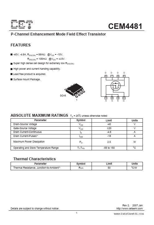
CEM4481 Key Features
- 40V, -4.6A, RDS(ON) = 66mΩ @VGS = -10V. RDS(ON) = 105mΩ @VGS = -4.5V. Super high dense cell design for extremely low RDS
CEM4481 is P-Channel Enhancement Mode Field Effect Transistor manufactured by CET.
| Part Number | Description |
|---|---|
| CEM4487 | P-Channel Enhancement Mode Field Effect Transistor |
| CEM4401 | P-Channel MOSFET |
| CEM4435A | P-Channel Enhancement Mode Field Effect Transistor |
| CEM4450 | N-Channel MOSFET |
| CEM4063 | p- |
P-Channel Enhancement Mode Field Effect Transistor.