CEP4301 Overview
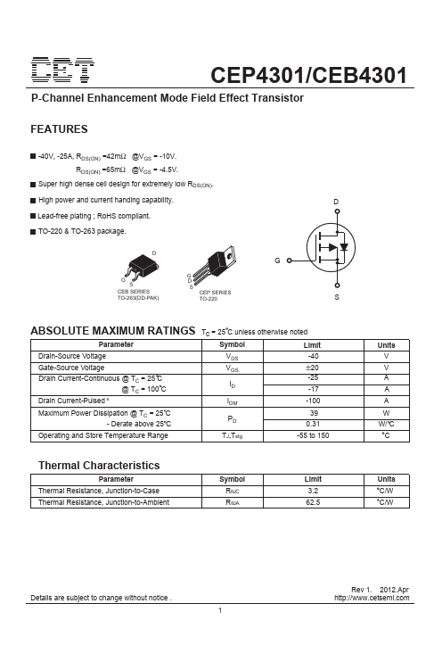
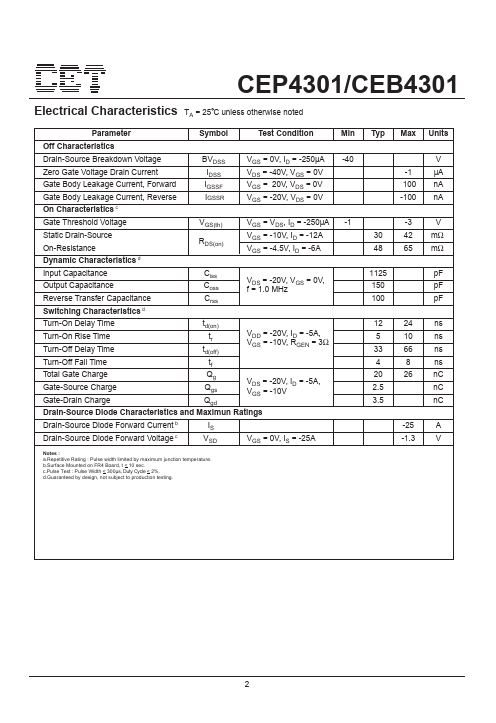
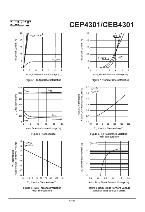
CEP4301/CEB4301 P-Channel Enhancement Mode Field Effect Transistor.
CEP4301 datasheet by CET.
| Part number | CEP4301 |
|---|---|
| Datasheet | CEP4301-CET.pdf |
| File Size | 391.59 KB |
| Manufacturer | CET |
| Description | P-Channel MOSFET |
|
|
CEP4301/CEB4301 P-Channel Enhancement Mode Field Effect Transistor.
| Part Number | Description |
|---|---|
| CEP41A2 | N-Channel MOSFET |
| CEP45N10 | N-Channel MOSFET |
| CEP01N6 | N-Channel MOSFET |
| CEP01N65 | N-Channel MOSFET |
| CEP01N6G | N-Channel MOSFET |
| CEP02N65A | N-Channel Enhancement Mode Field Effect Transistor |
| CEP02N65D | N-Channel MOSFET |
| CEP02N65G | N-Channel Enhancement Mode Field Effect Transistor |
| CEP02N6A | N-Channel MOSFET |
| CEP02N6G | N-Channel MOSFET |