CEP655N
CEP655N is N-Channel MOSFET manufactured by CET.
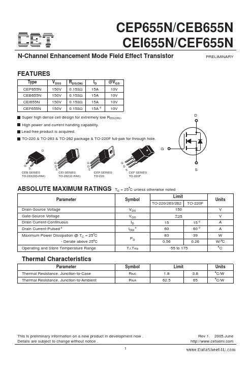
FEATURES
Type CEP655N CEB655N CEI655N CEF655N VDSS 150V 150V 150V 150V RDS(ON) 0.153Ω 0.153Ω 0.153Ω 0.153Ω ID 15A 15A 15A 15A d
PRELIMINARY
@VGS 10V 10V 10V 10V D
Super high dense cell design for extremely low RDS(ON). High power and current handing capability. Lead free product is acquired. TO-220 & TO-263 & TO-262 package & TO-220F full-pak for through hole.
S CEB SERIES TO-263(DD-PAK)
CEI SERIES TO-262(I2-PAK)
CEP SERIES TO-220
CEF SERIES TO-220F
ABSOLUTE MAXIMUM RATINGS
Parameter Drain-Source Voltage Gate-Source Voltage Drain Current-Continuous Drain Current-Pulsed a
Tc = 25 C unless otherwise noted Limit Symbol TO-220/263/262 VDS VGS ID IDM PD TJ,Tstg e
TO-220F
Units V V
±25
15 60 83 0.56 -55 to 175 15 60 39 0.26 d d
A A W W/ C C
Maximum Power Dissipation @ TC = 25 C
- Derate above 25 C Operating and Store Temperature Range
Thermal Characteristics
Parameter Thermal Resistance, Junction-to-Case Thermal Resistance, Junction-to-Ambient Symbol RθJC RθJA 1.8 62.5 Limit 3.8 65 Units C/W C/W
This is preliminary information on a new product in development now . Details are subject to change without notice . 1
Rev 1. 2005.June http://.cetsemi.
CEP655N/CEB655N CEI655N/CEF655N
Electrical Characteristics
Parameter Off Characteristics Drain-Source Breakdown Voltage Zero Gate Voltage Drain Current Gate Body Leakage Current, Forward Gate Body Leakage Current, Reverse On Characteristics b Gate Threshold Voltage Static Drain-Source On-Resistance Forward Transconductance Dynamic Characteristics Input Capacitance Output Capacitance Reverse Transfer Capacitance Switching Characteristics c Turn-On Delay Time Turn-On Rise Time Turn-Off Delay Time Turn-Off Fall Time Total Gate Charge Gate-Source Charge Gate-Drain Charge Drain-Source Diode Forward Current Drain-Source Diode Forward Voltage b c
Tc = 25 C unless otherwise noted Symbol BVDSS IDSS IGSSF IGSSR VGS(th) RDS(on) g FS Ciss Coss Crss td(on) tr td(off) tf Qg Qgs Qgd IS f VSD...