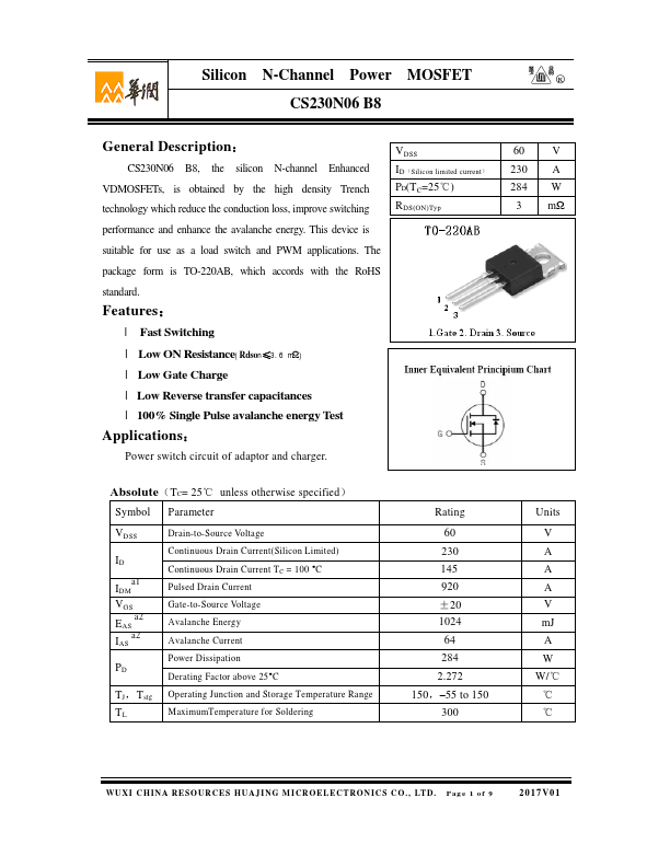
GENERAL DESCRIPTION
: CS230N06 B8, the silicon N-channel Enhanced VDMOSFETs, is obtained by the high density Trench technology which reduce the conduction loss, improve switching performance and enhance the avalanche energy. FEATURES
: l Fast Switching l Low ON Resistance(Rdson≤3.6 mΩ) l Low Gate Charge l Low Reverse transfer capacitances l 100% Single Pulse avalanche energy Test APPLICATIONS
: Power switch circuit of adaptor and charger. VDSS ID(Silicon limited current) PD(TC=25℃) RDS(ON)Typ 60 V 230 A 284 W 3 mΩ Absolute(TC= 25℃ unless otherwise specified) Symbol Parameter VDSS ID IDMa1 VGS EAS a2 IAS a2 PD TJ,Tstg TL Drain-to-Source Voltage Continuous Drain Current(Silicon Limited) Continuous Drain Current TC = 100 °C Pulsed Drain Current Gate-to-Source Voltage Avalanche Energy Avalanche Current Power Dissipation Derating Factor above 25°C Operating Junction and Storage Temperature Range MaximumTemperature for Soldering Rating 60 230 145 920 ±20 1024 64 284 2.272 150,–55 to 150 300 Units V A A A V mJ A W W/℃ ℃ ℃ WUXI CHI NA RESOURCES HUAJ I NG M I CROELECTRONI CS C O. , LTD. CR Micro