HGD032N03A Datasheet Text
Silicon N-Channel Power MOSFET
○R
HGD032N03A
General Description
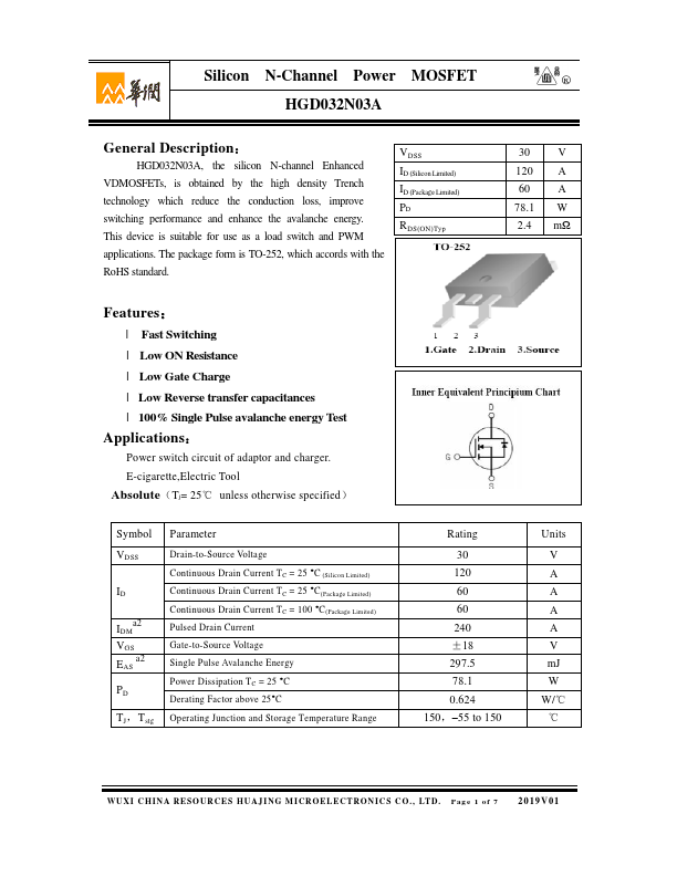
:
HGD032N03A, the silicon N-channel Enhanced VDMOSFETs, is obtained by the high density Trench technology which reduce the conduction loss, improve switching performance and enhance the avalanche energy. This device is suitable for use as a load switch and PWM applications. The package form is TO-252, which accords with the RoHS standard.
VDSS ID (Silicon Limited) ID (Package Limited) PD RDS(ON)Typ
30 V 120 A 60 A 78.1 W 2.4 mΩ
Features
: l Fast Switching l Low ON Resistance l Low Gate Charge l Low Reverse transfer capacitances l 100% Single Pulse avalanche energy Test
Applications:
Power switch circuit of adaptor and charger. E-cigarette,Electric Tool
Absolute(Tj= 25℃ unless otherwise specified)
Symbol VDSS
ID
IDMa2 VGS EAS a2 PD TJ,Tstg
Parameter
Drain-to-Source Voltage Continuous Drain Current TC = 25 °C (Silicon Limited) Continuous Drain Current TC = 25 °C(Package Limited) Continuous Drain Current TC = 100 °C(Package Limited) Pulsed Drain Current Gate-to-Source Voltage Single Pulse Avalanche Energy Power Dissipation TC = 25 °C Derating Factor above 25°C Operating Junction and Storage Temperature Range
Rating
30 120 60 60 240 ±18 297.5 78.1 0.624 150,- 55 to 150
Units
V A A A A V mJ W W/℃ ℃
WUXI CHI NA RESOURCES HUAJ I NG M I CROELECTRONI CS C O., LTD. Pag e 1 of 7 2 019V01
HGD032N03A
○R
Electrical Characteristics(Tj= 25℃ unless otherwise specified):
OFF Characteristics
Symbol
Parameter
Test Conditions
VDSS IDSS IGSS(F) IGSS(R)...