MTBA6C12J4
MTBA6C12J4 is N & P-Channel Enhancement Mode Power MOSFET manufactured by CYStech.
CYStech Electronics Corp.
Spec. No. : C973J4 Issued Date : 2014.06.13 Revised Date : 2014.10.02 Page No. : 1/13
N & P-Channel Enhancement Mode Power MOSFET
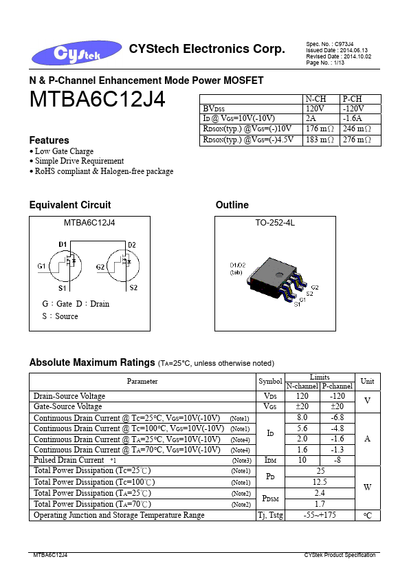
MTBA6C12J4 BVDSS
ID @ VGS=10V(-10V)
RDSON(typ.) @VGS=(-)10V
Features
RDSON(typ.) @VGS=(-)4.5V
- Low Gate Charge
- Simple Drive Requirement
- RoHS pliant & Halogen-free package
N-CH 120V 2A 176 mΩ
183 mΩ
P-CH -120V -1.6A 246 mΩ
276 mΩ
Equivalent Circuit
Outline
TO-252-4L
G:Gate D:Drain...