Datasheet4U.com
🌙
MTN2302V3 Datasheet | CYStech
Part:
MTN2302V3
Description:
N-Channel Enhancement Mode MOSFET
Category:
MOSFET
Manufacturer:
CYStech
Size:
338.67 KB
MTN2302V3 Datasheet (PDF) Download
Related MTN2302V3 Datasheets
MTN2302S3 N-Channel Enhancement Mode MOSFET
MTN2302N3 N-Channel Enhancement Mode MOSFET
CYStech
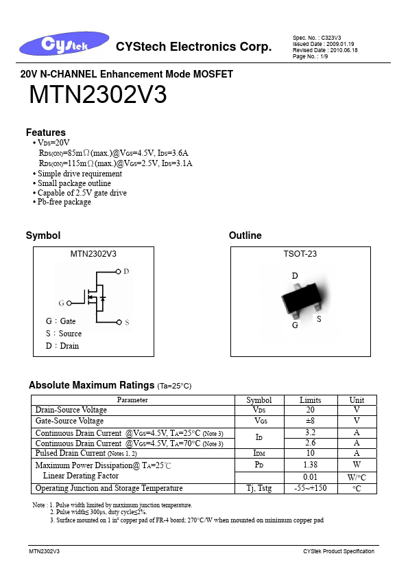
MTN2302V3
Key Features
VDS=20V RDS(ON)=85mΩ(max.)@VGS=4.5V, IDS=3.6A RDS(ON)=115mΩ(max.)@VGS=2.5V, IDS=3.1A
Simple drive requirement
Small package outline
Capable of 2.5V gate drive
Pb-free package
×
Close