Datasheet Summary
Dual N-Channel JFET High Frequency Amplifier
CORPORATION
2N5911 / 2N5912
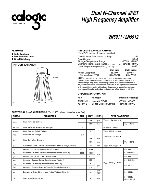
Features...
| Manufacturer | Part Number | Description |
|---|---|---|
| 2N5911 | N-CHANNEL JFET | |
| 2N5911 | dual n-channel JFET | |
| 2N5911 | Dual Matched N-Channel JFET | |
| 2N5911 | N-Channel Monolithic Dual JFET |