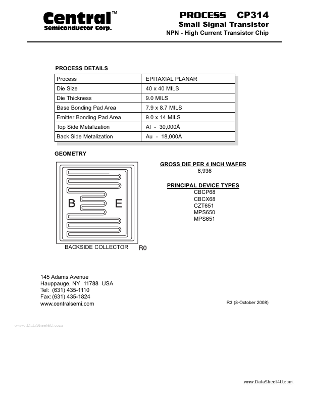
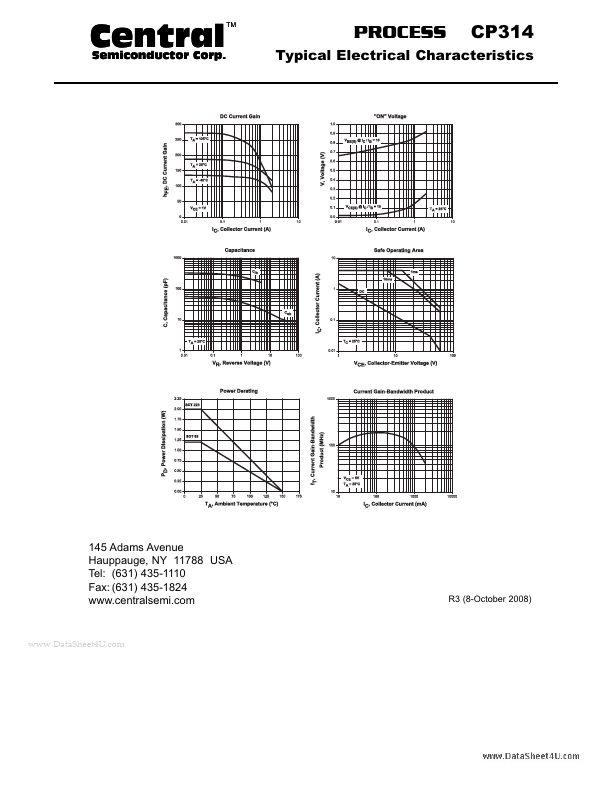
CP314 Description
Central TM PROCESS CP314 Semiconductor Corp. (631) 435-1824 .centralsemi. Central TM PROCESS CP314 Semiconductor Corp.
CP314 is Small Signal Transistor NPN - High Current Transistor Chip manufactured by Central Semiconductor .
| Part Number | Description |
|---|---|
| CP310 | Small Signal Transistor NPN - High Voltage Transistor Chip |
| CP312 | Power Transistor NPN - Amp/Switch Transistor Chip |
| CP315V | Power Transistors NPN - High Current Transistor Chip |
| CP316V | Small Signal Transistors NPN - High Voltage Transistor Chip |
| CP317 | Small Signal Transistor NPN - RF Transistor Chip |
Central TM PROCESS CP314 Semiconductor Corp. (631) 435-1824 .centralsemi. Central TM PROCESS CP314 Semiconductor Corp.