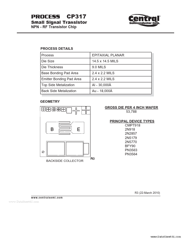
CP317 Description
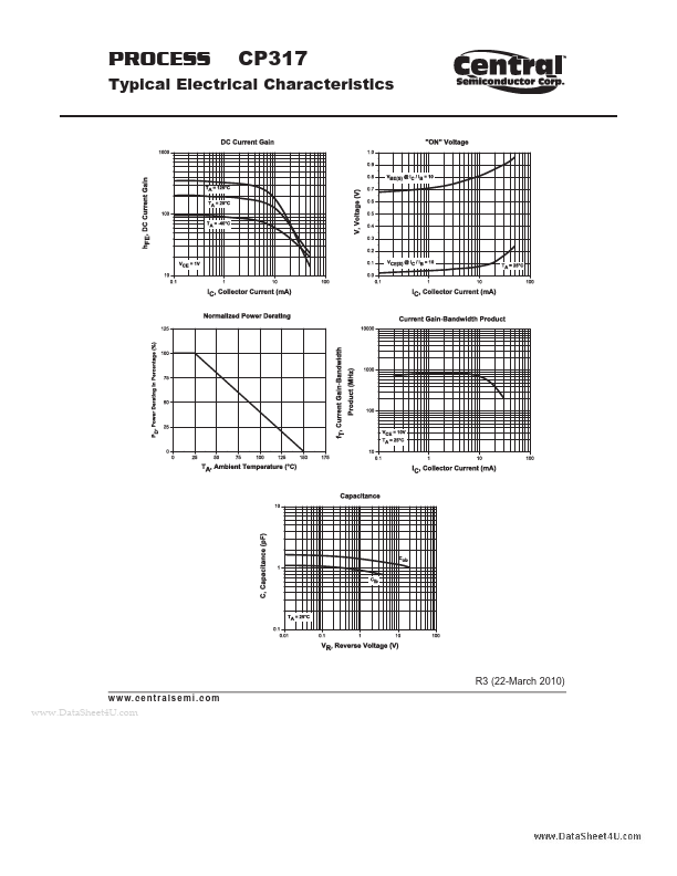
PROCESS CP317 Typical R3 (22-March 2010) w w.
CP317 Key Features
- s e m i . c o m .. PROCESS CP317 Typical
CP317 is Small Signal Transistor NPN - RF Transistor Chip manufactured by Central Semiconductor .
| Part Number | Description |
|---|---|
| CP317V | Small Signal Transistor |
| CP310 | Small Signal Transistor NPN - High Voltage Transistor Chip |
| CP312 | Power Transistor NPN - Amp/Switch Transistor Chip |
| CP314 | Small Signal Transistor NPN - High Current Transistor Chip |
| CP315V | Power Transistors NPN - High Current Transistor Chip |
PROCESS CP317 Typical R3 (22-March 2010) w w.