CP382X Description
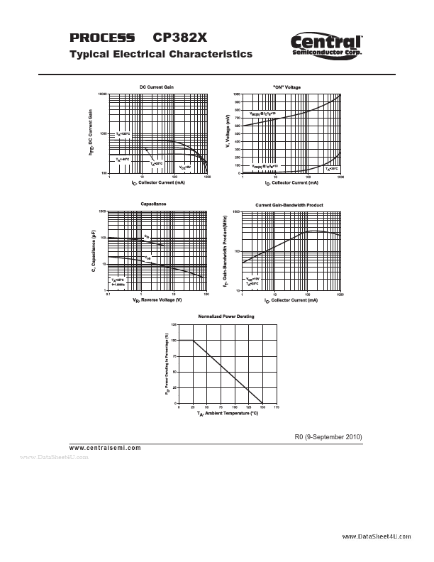
PROCESS CP382X Typical R0 (9-September 2010) w w.
CP382X Key Features
- s e m i . c o m .. PROCESS CP382X Typical
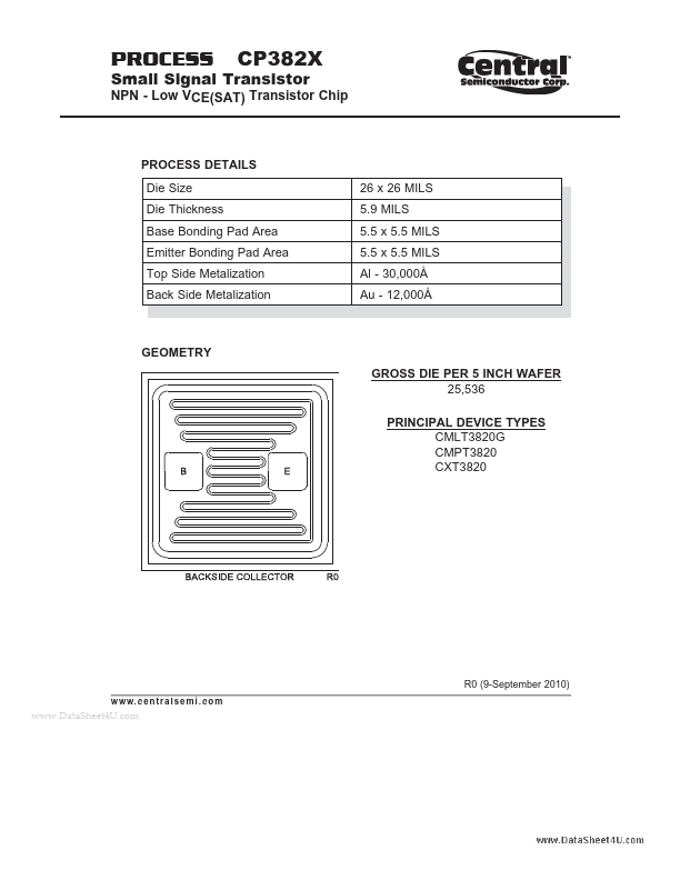
CP382X is Small Signal Transistor NPN - Low VCE(SAT) Transistor Chip manufactured by Central Semiconductor .
| Part Number | Description |
|---|---|
| CP302-MPSH10 | NPN - RF Transistor Die |
| CP305 | Small Signal Transistor NPN - High Current Transistor Chip |
| CP305V-BCW66H | NPN Transistor |
| CP307 | Small Signal Transistor NPN - Silicon Darlington Transistor Chip |
| CP309 | Power Transistor NPN - Low Saturation Transistor Chip |
PROCESS CP382X Typical R0 (9-September 2010) w w.