CP394R
CP394R is N-Channel MOSFET manufactured by Central Semiconductor.
PROCESS
Small Signal MOSFET Transistor
N-Channel Enhancement-Mode Transistor Chip
..
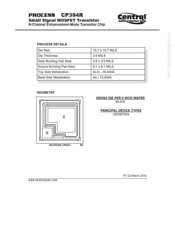
PROCESS DETAILS Die Size Die Thickness Gate Bonding Pad Area Source Bonding Pad Area Top Side Metalization Back Side Metalization 15.7 x 15.7 MILS 3.9 MILS 3.9 x 3.9 MILS 9.1 x 8.1 MILS Al-Si
- 35,000Å Au
- 12,000Å
GEOMETRY GROSS DIE PER 6 INCH WAFER 95,400 PRINCIPAL DEVICE TYPES CEDM7004
R1 (22-March 2010) w w w. c e n t r a l s e m i . c o m
PROCESS
Typical Electrical Characteristics
R1 (22-March 2010) w w w. c e n t r a l s e m i . c o...