CP753V
CP753V is PNP Transistor manufactured by Central Semiconductor.
PROCESS
Small Signal Transistors
- High Current Transistor Chip
..
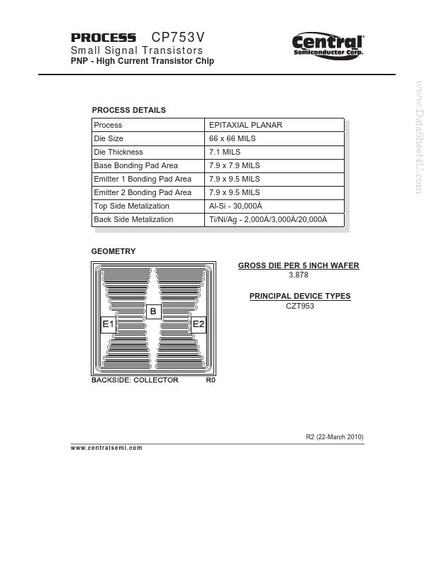
PROCESS DETAILS Process Die Size Die Thickness Base Bonding Pad Area Emitter 1 Bonding Pad Area Emitter 2 Bonding Pad Area Top Side Metalization Back Side Metalization EPITAXIAL PLANAR 66 x 66 MILS 7.1 MILS 7.9 x 7.9 MILS 7.9 x 9.5 MILS 7.9 x 9.5 MILS Al-Si
- 30,000Å Ti/Ni/Ag
- 2,000Å/3,000Å/20,000Å
GEOMETRY GROSS DIE PER 5 INCH WAFER 3,878 PRINCIPAL DEVICE TYPES CZT953
R2 (22-March 2010) w w w. c e n t r a l s e m i . c o m
PROCESS
Typical Electrical Characteristics
R2 (22-March 2010) w w w. c e n t r a l s e m i . c o...