CED61A3
CED61A3 is N-Channel MOSFET manufactured by Chino-Excel Technology.
- Part of the CED61A3-Chino comparator family.
- Part of the CED61A3-Chino comparator family.
FEATURES
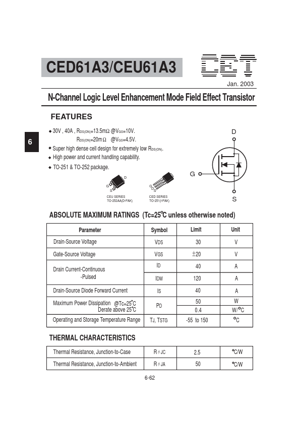
30V , 40A , RDS(ON)=13.5mΩ @VGS=10V. RDS(ON)=20m Ω @VGS=4.5V. Super high dense cell design for extremely low RDS(ON). High power and current handling capability. TO-251 & TO-252 package.
CEU SERIES TO-252AA(D-PAK)
CED SERIES TO-251(l-PAK)
ABSOLUTE MAXIMUM RATINGS (Tc=25 C unless otherwise noted)
Parameter Drain-Source Voltage Gate-Source Voltage Drain Current-Continuous -Pulsed Drain-Source Diode Forward Current Maximum Power Dissipation @Tc=25 C Derate above 25 C Operating and Storage Temperature Range Symbol VDS VGS ID IDM IS PD TJ, TSTG Limit 30 Unit V V A A A W W/ C C
Ć20
40 120 40 50 0.4 -55 to 150
THERMAL CHARACTERISTICS
Thermal Resistance, Junction-to-Case Thermal Resistance, Junction-to-Ambient RįJC RįJA
6-62
2.5 50
C/W C/W
CED61A3/CEU61A3
ELECTRICAL CHARACTERISTICS (TC= 25 C unless otherwise noted)
Parameter OFF CHARACTERISTICS
Drain-Source Breakdown Voltage Zero Gate Voltage Drain Current Gate-Body Leakage BVDSS IDSS IGSS VGS(th) RDS(ON) ID(ON) g FS b
Symbol
Condition
VGS = 0V, ID=250µA VDS = 30V, VGS = 0V VGS = Ć20V, VDS = 0V VDS = VGS, ID 250µA VGS = 10V, ID = 20A VGS = 4.5V, ID = 18A VDS = 10V, VGS = 10V VDS = 10V, ID = 26A
Min Typ Max Unit
30 1 Ć100 1 11 16.5 40 34 1200 480 130 3 V µA n A V mΩ A S
PF PF PF
ON CHARACTERISTICS a
Gate Threshold Voltage Drain-Source On-State Resistance On-State Drain Current Forward Transconductance 13.5 mΩ 20
DYNAMIC CHARACTERISTICS
Input Capacitance Output Capacitance Reverse Transfer Capacitance
CISS COSS CRSS b
VDS =15V, VGS = 0V f =1.0MHZ
SWITCHING CHARACTERISTICS
Turn-On Delay Time Rise Time Turn-Off Delay Time Fall Time Total Gate Charge Gate-Source Charge Gate-Drain Charge t D(ON) tr t D(OFF) tf Qg Qgs Qgd
VDD = 15V, ID = 40A, VGS = 10V RGEN =24Ω VDS = 15V,ID = 40A VGS = 5V
18 25 45 75 19 5 9
30 50 90 130 23 ns ns ns ns n C n C n...