Datasheet4U Logo Datasheet4U.com

CEM8206 - Dual N-Channel MOSFET

Download the CEM8206 datasheet PDF. This datasheet also covers the CEM8206-Chino variant, as both devices belong to the same dual n-channel mosfet family and are provided as variant models within a single manufacturer datasheet.

Key Features

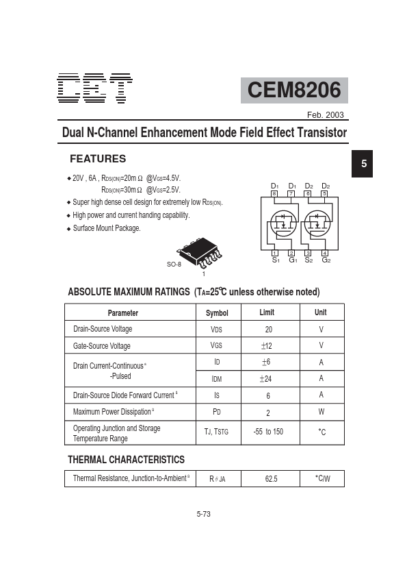
  • 20V , 6A , RDS(ON)=20m Ω @VGS=4.5V. RDS(ON)=30m Ω @VGS=2.5V. Super high dense cell design for extremely low RDS(ON). High power and current handing capability. Surface Mount Package. 1 2 3 4 5 D1 8 D1 7 D2 6 D2 5 SO-8 1 S1 G1 S2 G2.

📥 Download Datasheet

Note: The manufacturer provides a single datasheet file (CEM8206-Chino-ExcelTechnology.pdf) that lists specifications for multiple related part numbers.

Datasheet Details

Part number CEM8206
Manufacturer Chino-Excel Technology
File Size 57.06 KB
Description Dual N-Channel MOSFET
Datasheet download datasheet CEM8206 Datasheet

Full PDF Text Transcription for CEM8206 (Reference)

Note: Below is a high-fidelity text extraction (approx. 800 characters) for CEM8206. For precise diagrams, and layout, please refer to the original PDF.

CEM8206 Feb. 2003 Dual N-Channel Enhancement Mode Field Effect Transistor FEATURES 20V , 6A , RDS(ON)=20m Ω @VGS=4.5V. RDS(ON)=30m Ω @VGS=2.5V. Super high dense cell desi...

View more extracted text
)=20m Ω @VGS=4.5V. RDS(ON)=30m Ω @VGS=2.5V. Super high dense cell design for extremely low RDS(ON). High power and current handing capability. Surface Mount Package. 1 2 3 4 5 D1 8 D1 7 D2 6 D2 5 SO-8 1 S1 G1 S2 G2 ABSOLUTE MAXIMUM RATINGS (TA=25 C unless otherwise noted) Parameter Drain-Source Voltage Gate-Source Voltage Drain Current-Continuous a -Pulsed Drain-Source Diode Forward Current a Maximum Power Dissipation a Operating Junction and Storage Temperature Range Symbol VDS VGS ID IDM IS PD TJ, TSTG Limit 20 Unit V V A A A W C Ć12 Ć6 Ć24 6 2 -55 to 150 THERMAL CHARACTERISTICS Thermal Resistance, Junction-to-Ambient a